Electronic Circuits - interfacing with a Z80 microprocessor v10 (PCB build)
My seb80 custom computer now has its own page here
This is version 10 of my Z80 interfacing project. My goal in this version was to manufacture the computer on PCBs.
I have named this computer seb80
Previous versions:
I have named this computer seb80
Previous versions:
- version 1 - initial wire-up, executes NOPs, observe incrementing address
- version 2 - experiment with and observe machine cycles M2 (memory read) and M3 (memory write)
- version 3 - address and data buses
- version 4 - introduce ROM and run program from it
- version 5 - introduce RAM
- version 6 - oscillator clock, NMI button, and INT/NMI tests
- version 7 - I/O output device
- version 8 - I/O input device
- version 9 - NTSC analog video signal generation
This version took me significantly longer than prior ones. Most of the work here was split between planning PCB layout and actually soldering the computer.
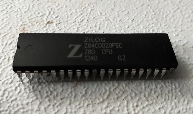
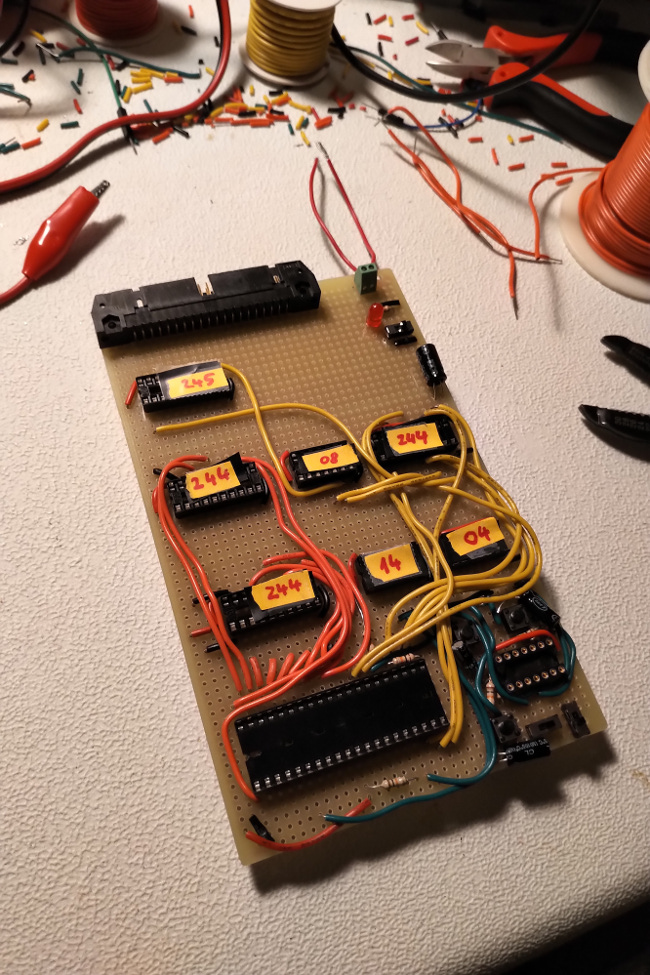
All ICs are placed in sockets, to make it easy to replace if they get damaged. I've used higher-quality machined sockets for those which might be replaced more routinely: the ROM and the oscillator.
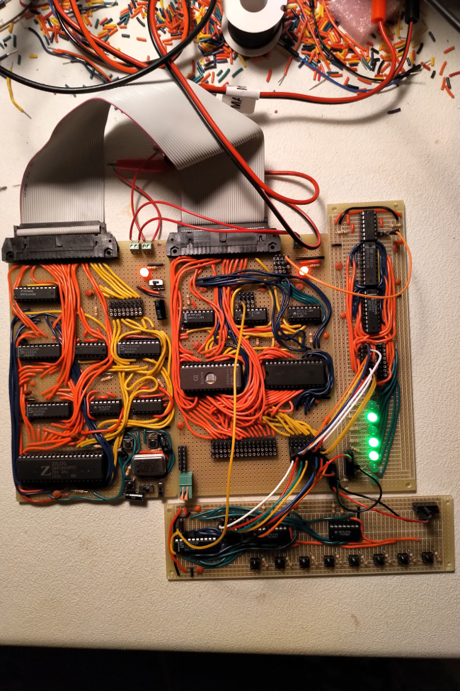
The computer proper is made up of two boards: CPU board and memory/expansion board. The computer also has built-in 4 input device selectors and 4 output device selectors, to reduce the amount of external circuitry needed for these first 8 devices.
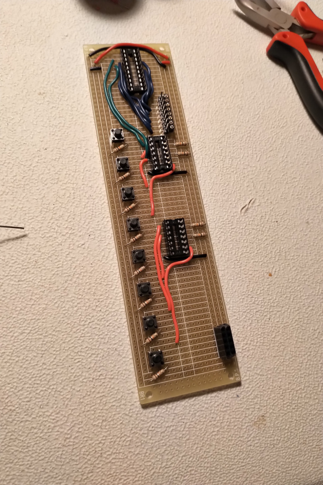
I've built two simple devices on their own PCBs. One is a latch/interface board. It latches data written to it via OUT instructions, making it available to a consumer device via a set of pin headers. Eight on-board LEDs display this latched data, which makes the board useful for debugging, as well.
The second device is a minimalistic keyboard, which uses 8 push buttons. 7 bits are available to compose a "key", while the last button is used as a latch. ROM software reads in the 7 bits only when the latch bit goes high (is pressed).
At this time, its ROM (version 0) simply writes to the output device whenever a value is latched by the user on the keyboard.
ROM version 0 binary
ROM version 0 source


Log
day 1The crystal oscillator needs its own power switch, or it freezes the CPU, even if not connected to the clock pin.
Started designing the CPU PCB.
I'm using electrical tape to fix IC sockets and switches onto the PCB first.
I've started with the CPU and clock.
day 2
Work continues on planning the layout of the CPU PCB.
I've decided to use higher-quality (and more expensive) machined sockets for the ICs that will be more often removed and re-inserted (such as EPROM and oscillator).
day 3
The layout is mostly decided on and soldering has begun.
I'm starting with the CPU board, which is the more difficult one - due to the multitude of connections.
I've started with the clock, reset, and NMI circuits.
day 4
Soldering continues.
The clock, reset, and NMI circuits are all connected to the 40-pin Z80 socket.
Soldered all IC sockets entirely.
Also soldered edge connector entirely. It was difficult due to everything being so close together and having to jump traces.
Burned my fingers twice and stabbed one deeply enough to bleed.
day 5
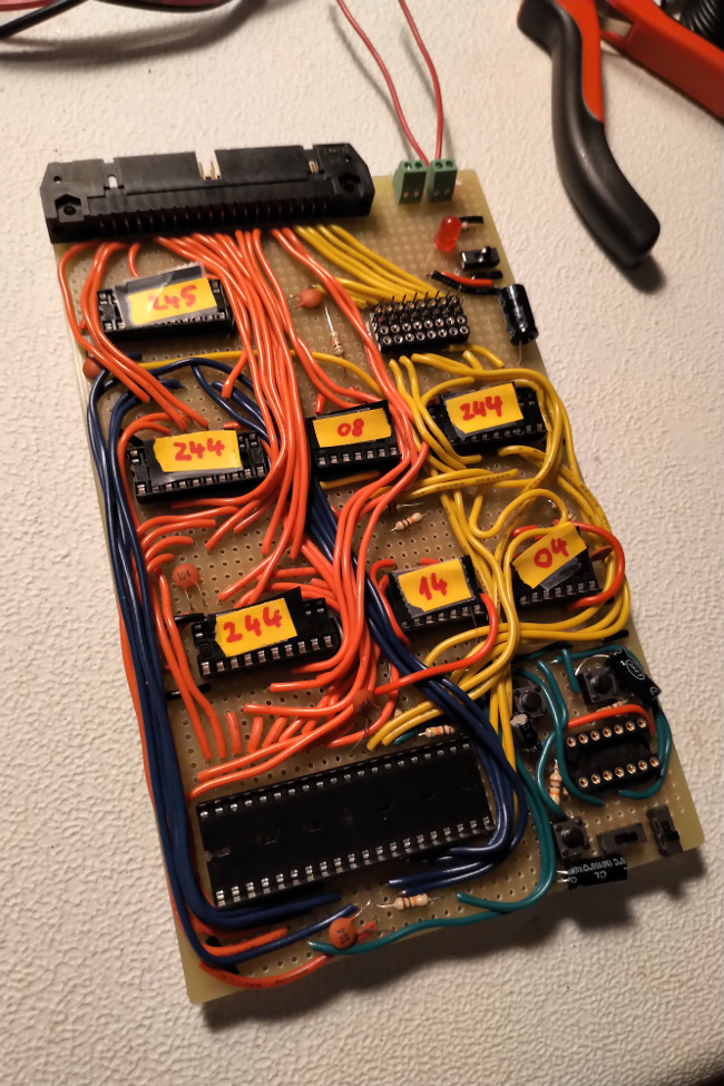
More soldering, moved on to CPU's control lines.
day 6
More soldering, moved on to CPU's address lines.
day 7
More soldering, the CPU control (output) lines are now connected all the way to the edge connector.
I have decided to bring the pin headers (for external connections) onto the CPU board, since it was not only convenient, but I had some spare room on it.
This also reduces the amount of wires running across the secondary (memory/extension) board by 20-25%.
day 8
More soldering, moved on to CPU's data lines.
day 9
More soldering, moved on to bringing the address lines to the edge connector.
day 10
With the addition of a few bypass capacitors, the CPU board is complete for now.
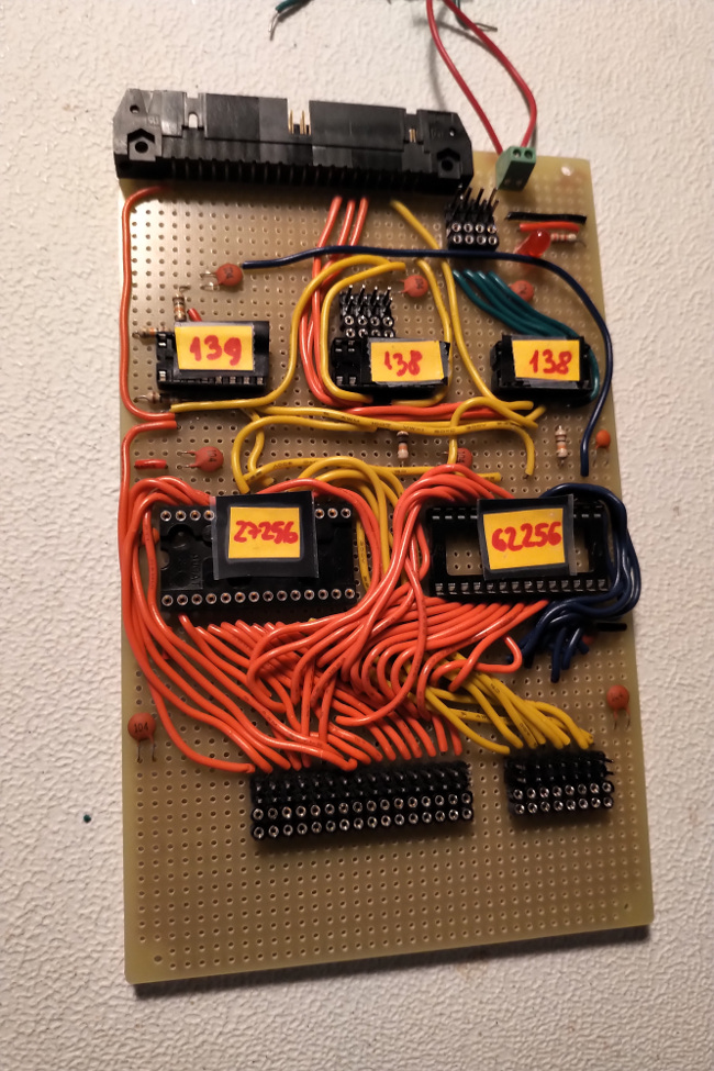
I'm moving on to the memory/expansion board.
Soldered the edge connector and all IC sockets on the memory/expansion board.
day 11
Another day of soldering, another bloody finger.
Started with all bypass capacitors, since I think it's easier to add them first, to run all wires on top of them, as they lay flat.
Moved on to memory chip and I/O device selectors.
Soldered all inputs to the selectors, as well as all control lines for RAM and ROM.
day 12
Updated diagram with PCB details (connectors, etc.)
Started preparing all pin headers for the expansion points (2 male and 2 female pins for each address line, data line, 4 input devices, 4 output devices).
day 13
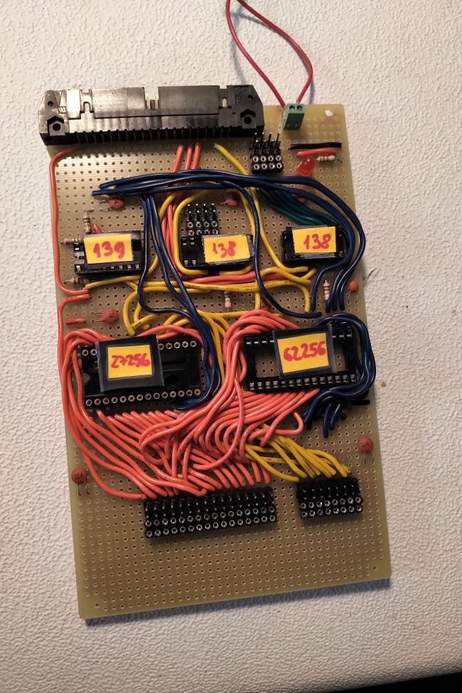
Finished preparation of pin headers; I now have all necessary segments.
Soldered address and data expansion pin headers. It was stressful, since there was such a high density of connections.
Soldered ROM to expansion.
The plan is to solder RAM to expansion, and then ROM to edge connector.
day 14
Ceramic disc capacitors have very sharp pins. I found this out while getting another bloody finger.
Soldered RAM to expansion.
Soldered the 4 input device selectors and 4 output device selectors.
Added all connectors to diagram.
day 15
Soldered RAM and ROM to edge connector, which connects all components to the address and data buses.
Added a few power connectors for any external devices to be supplied easily.
Added a PCB layout diagram to the overall diagram.
day 16
These IC sockets are strong. The RAM one gave me 5 inline stabs while trying to pry the IC out of it.
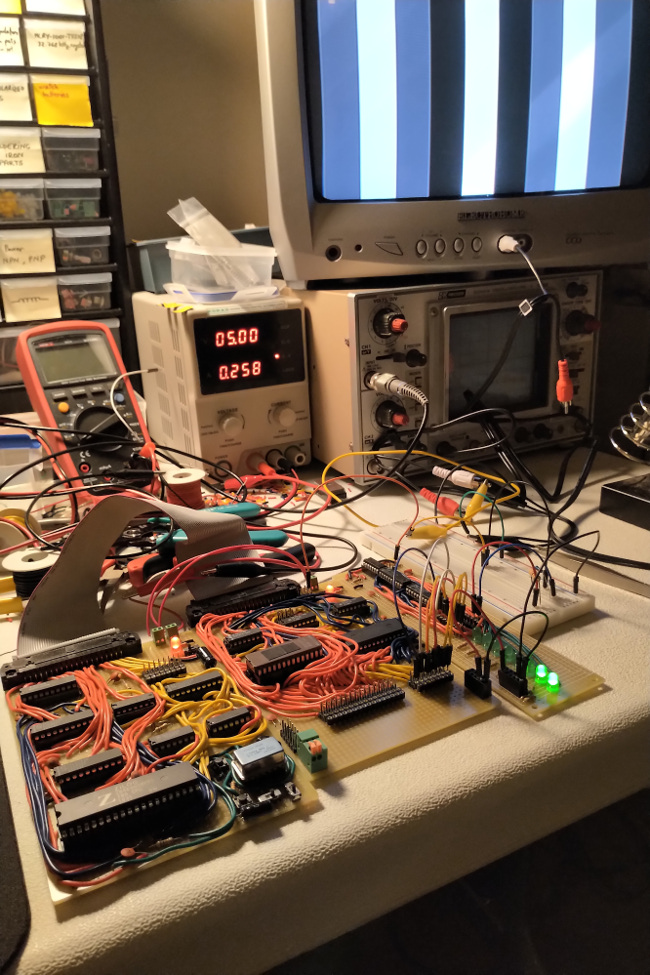
The time I spent carefully checking all connections has paid off: the computer worked "out of the box"!
My first test was with a simple infinite loop at address 0: JP 0
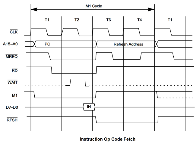
I was able to match the M1/RD timing I observed on the oscilloscope, with one I recorded earlier.
The one from before used a 0.1 MHz clock; its edges were clean, and its high/low levels stable.
This one uses a 3.63 MHz clock; its edges are clearly affected by stray capacitance. Its high/low levels are impacted by - most likely - crosstalk in the ribbon cable, showing as much as a 0.5 V fluctuation in what should be constant high level voltage. Low level fluctuation is smaller, at around 0.3 V.
I'm glad the TTL standard has enough slack built in.
New issue: IORQ, WR seem to not output correctly, staying high past the 74LS244 buffer. This causes the I/O output device selector to not function at all.
This took a few hours to troubleshoot, and it was a combination of issues.
First, IORQ and WR did output correctly. It was just impossible to see on the oscilloscope, as the low state lasted such a short time compared to everything else.
Second, latched output was in fact correct, although initially it seemed fast enough to mean that the latch was in its pass-through state at all times. The issue is that I had reused a program which I wrote (and tested) with a significantly slower clock speed (perhaps 1 kHz), whereas now the clock is at 3.6864 MHz. This and the above made it seem like the latch was always pass-through because IORQ and WR stayed high (inactive).
Third, to make things more difficult, I damaged a Z80 - most likely by discharging static electricity into it. The air in the room is quite dry this time of year. I have to be more careful around these CPUs.
Fourth, it seems like channel 2 of my oscilloscope is sometimes malfunctioning. For some reason it won't pick up voltage changes, except at high frequencies.
After a few modifications to the program, I can clearly see IORQ and WR on the oscilloscope as well.
day 17
Brought over the NTSC signal generation circuit and tested it successfully.
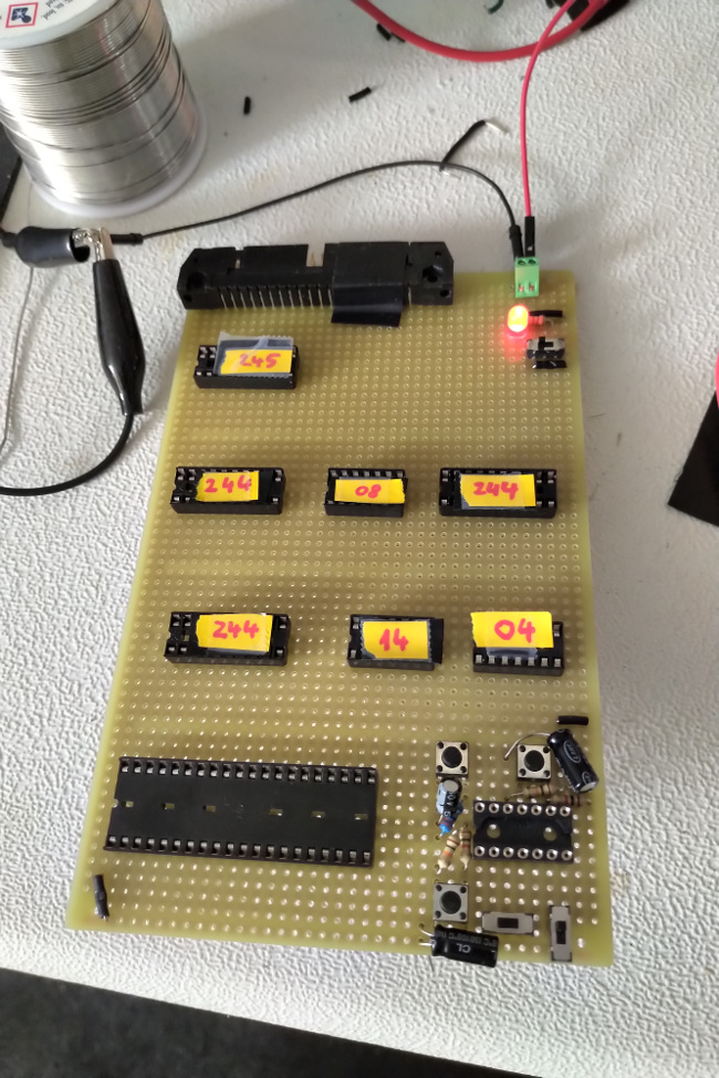
Next, I will create a latch device which can be used as a generic output device, based on the 74LS373. Its outputs will be buffered via a 74LS244.
Wasted an IC socket after choosing a cheap PCB whose traces had unintended contacts.
Decided to use a good PCB rather than a cheap one.
day 18
Finished soldering the latch device on a PCB.
This device offers 8-bit data output that is latched when a byte is written to its hardware I/O port.
Any consumer device can rely on this to receive data from the Z80 reliably.
Bonus: because I had room on the board, I also connected 8 LEDs to the outputs. This makes it excellent for debugging - for example, the value of the accumulator can be written to it and then observed by a human.
From the specs, the 74LS244 can source 15 mA from a logical high output pin (more from a logical low). I've measured the green LEDs at 2.3 V and they're in series with 2.2 kOhm. From the 74LS244's measured logical high of 3.2 V, the LEDs consume about 0.4 mA, leaving quite a bit for a low-power device to draw directly from this latch board.
day 19
Started work on the computer's first input device.
It's based on 8 push buttons, each hardware-debounced via a Schmitt trigger.
I expect to use one of the switches as the "latch", so that it's easy to interface this device by polling.
day 20
More soldering on the keyboard.
day 21
Finished soldering the keyboard.
Updated diagram.
day 22
The computer is now officially named seb80 (intentionally all lowercase). It sounds a bit like "zed eighty", the CPU.
Laid the foundation for seb80's ROM.
It will feature a collection of useful routines, including delays, keyboard, etc.
Wrote a keyboard routine which will register latches and return both whether something was just latched and current hardware button state.
This proves that the keyboard module works - and it works the first time!
I am very pleased that for the amount (I approximate around 1000 points) of soldering I have done, everything worked the first time; no soldering fix-ups were needed. Much of that is owed to the time I spent updating and verifying the diagram, as well as on-going continuity testing after each batch of connections I soldered.
day 23
Finished up ROM development for this version.
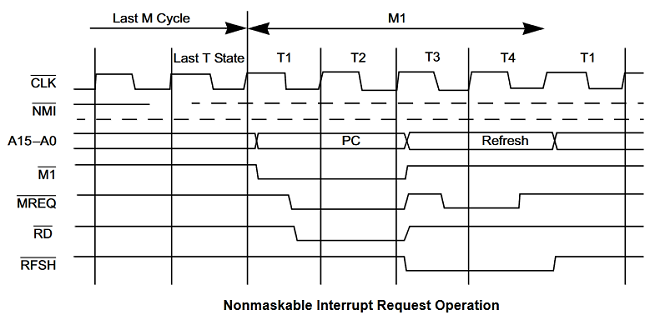
Z80 diagrams
Here are some useful diagrams, including the Z80 pinout, timing diagrams, etc.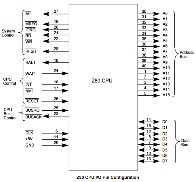


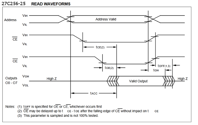
27C256 EPROM diagrams
Here are some useful diagrams, including pinout, timing, etc.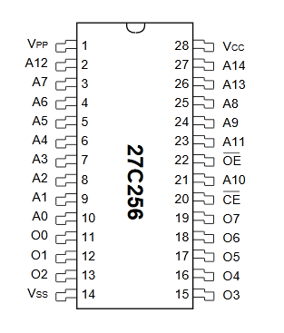
62256 RAM diagrams
Here are some useful diagrams, including pinout, timing, etc.

