Electronic Circuits - interfacing with a Z80 microprocessor v8 (input from I/O device)
My seb80 custom computer now has its own page here
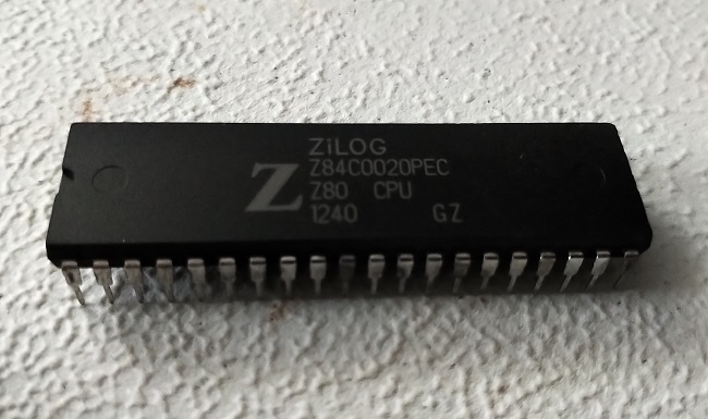
This is version 8 of my Z80 interfacing project. My goal in this version was to introduce an I/O input device, from which the CPU could read data via the IN instruction.
Previous versions:
Previous versions:
- version 1 - initial wire-up, executes NOPs, observe incrementing address
- version 2 - experiment with and observe machine cycles M2 (memory read) and M3 (memory write)
- version 3 - address and data buses
- version 4 - introduce ROM and run program from it
- version 5 - introduce RAM
- version 6 - oscillator clock, NMI button, and INT/NMI tests
- version 7 - I/O output device
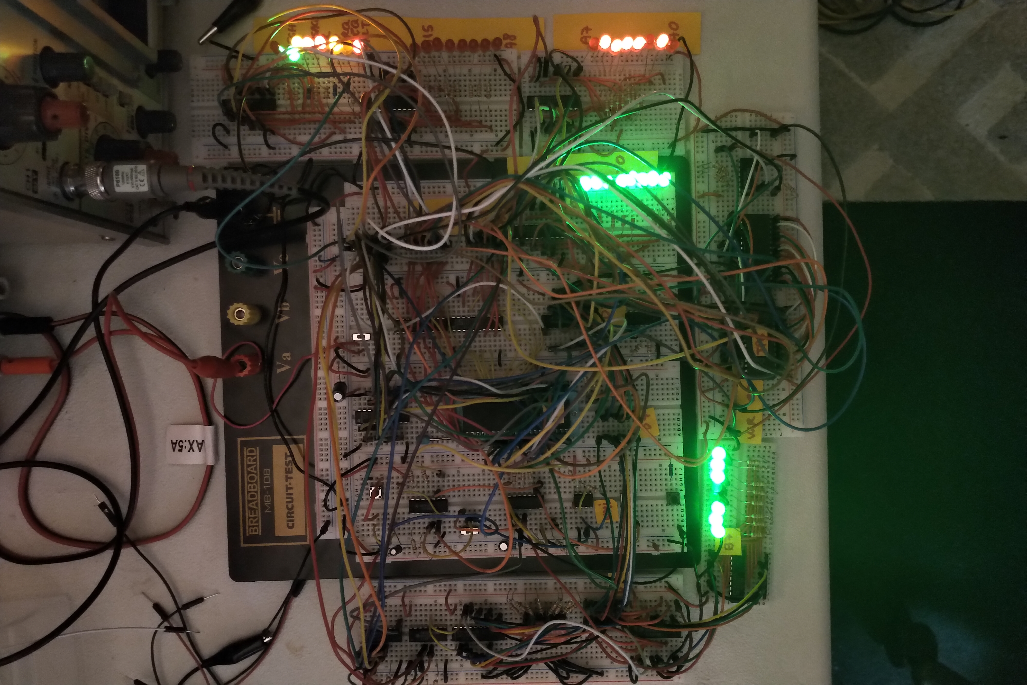
To create a way to input from a device, I used a second 74LS138 3-to-8 decoder as well as a 74LS244, which becomes enabled only when the specific device is read. When this happens, the 74LS244 gains control of the data bus, writing to it.
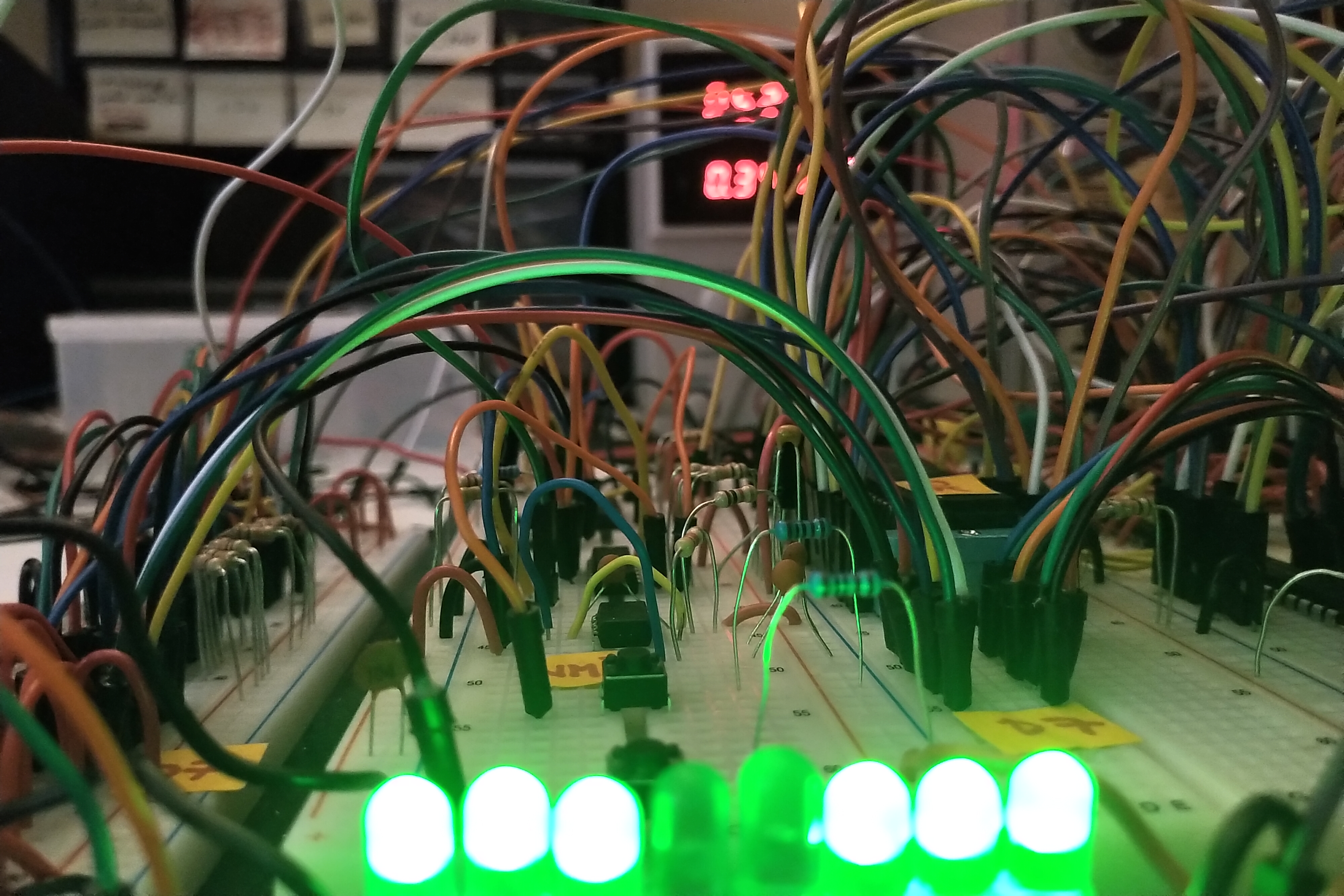
The input device I built is a segment of 8 DIP switches.
TP6 - test program for I/O input


Log
day 1This begins part 2 of interfacing with I/O devices; in this version I want to add the necessary circuitry to be able to input from devices.
Just like for output devices, a 74LS138 3-to-8 decoder (part is SN74LS138N) will be used to enable one of up to four input devices.
Already, I/O devices at port 4, 5, 6, 7 (A2=1) are be output devices.
Thus, I/O devices at port 0, 1, 2, 3 (A2=0) will be input devices.
NOTE: for input devices that won't rely on these built-in selectors, care has to be taken that they are wired to ports whose A2=1, to not conflict with the built-in input device selectors which expect A2=0.
Input devices:


A2  A1  A0

C   B   A  Y

0   0   0  Y0  input device at port 0

0   0   1  Y1  input device at port 1

0   1   0  Y2  input device at port 2

0   1   1  Y3  input device at port 3
day 2
The second 74LS138 was easy to design; it's just like the output one, except being enabled by Z80's RD line (along with IORQ).
The switches will be buffered by a 74LS244, enabled by one of the input device selector's outputs.
day 3
Wired up the input selector 74LS138.
Wrote TP6, a test program to test input via a device made up of switches:
Address  Bytes            Mnemonic

0000                      ; TP6

0000                      ; test program for I/O input

0000                      ;

0000                      ; the reason for these is to verify that

0000                      ; the input device selector remains inactive

0000                      ; during outputs

0000   3E 81              LD A, 10000001b

0002   D3 04              OUT (04h), A

0004   3E C3              LD A, 11000011b

0006   D3 05              OUT (05h), A

0008   3E E7              LD A, 11100111b

000A   D3 06              OUT (06h),A

000C   3E FF              LD A, 11111111b

000E   D3 07              OUT (07h),A

0010   3E 00              LD A, 0

0012   D3 06              OUT (06h), A  ; clear LEDs

0014                      ; now read from the four input devices, to

0014                      ; verify correct signals from the input

0014                      ; device selector

0014   DB 00              IN A, (00h)   ; reads garbage when not connected

0016   DB 01              IN A, (01h)   ; reads garbage when not connected

0018   DB 02              IN A, (02h)   ; reads garbage when not connected

001A            READ_SWITCHES:

001A   DB 03              IN A, (03h)   ; read switches

001C   D3 06              OUT (06h), A  ; display value on LEDs

001E   C3 1A 00           JP READ_SWITCHES
Verified that the 74LS138 correctly selects an input device, as wired.
Wired up the 74LS244. It was much easier than before, with the extensive wiring diagram I've been maintaining.
Program TP6 ran successfully, demonstrating the full I/O cycle (read from DIP switches, write to LEDs).
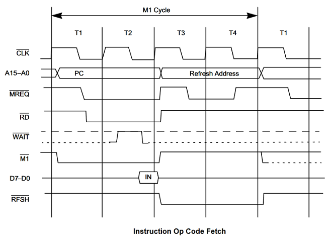
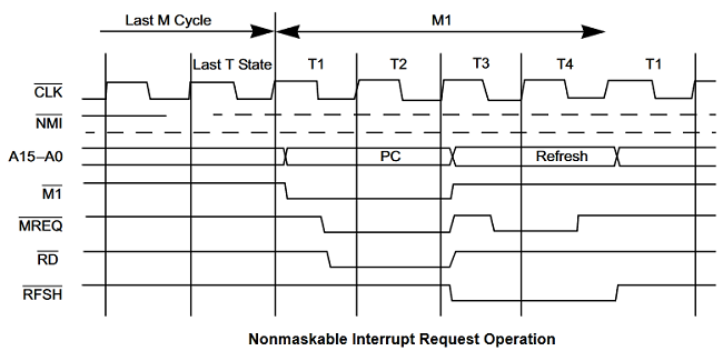
Z80 diagrams
Here are some useful diagrams, including the Z80 pinout, timing diagrams, etc.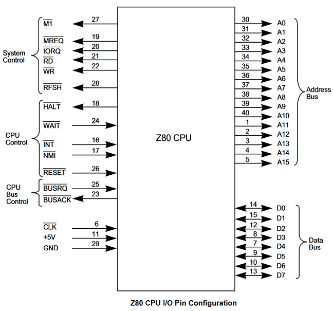


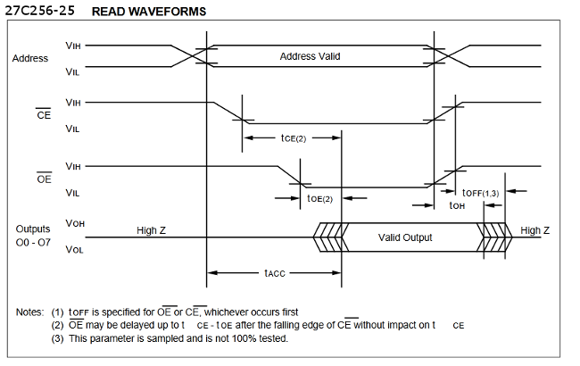
27C256 EPROM diagrams
Here are some useful diagrams, including pinout, timing, etc.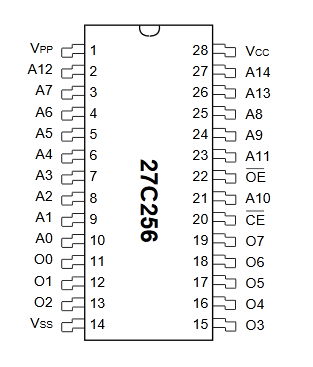
62256 RAM diagrams
Here are some useful diagrams, including pinout, timing, etc.

