Electronic Circuits - interfacing with a Z80 microprocessor v4 (introduce ROM)
My seb80 custom computer now has its own page here
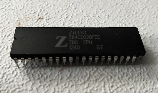
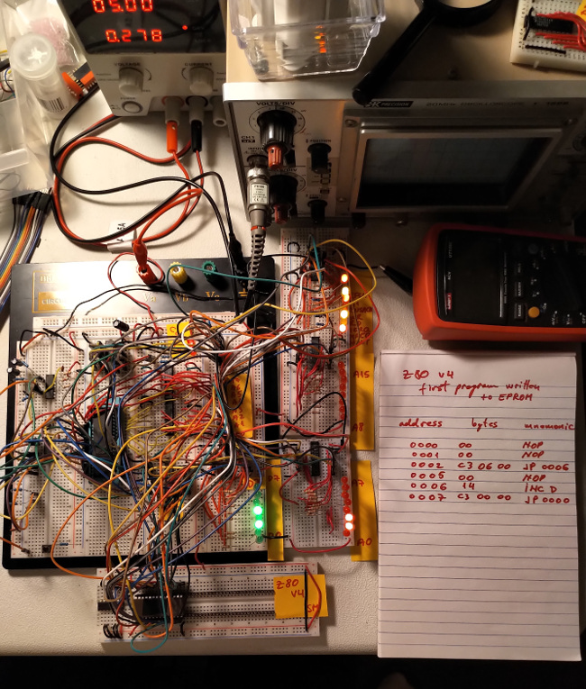
This is version 4 of my Z80 interfacing project. My goal here was to complete the address, data, and control buses and to add an EPROM from which to run a simple program.
Previous versions:
Previous versions:
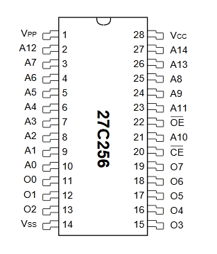
Version 4 is important because it introduces memory. To that end I used the 27C256-25 EPROM. Its capacity is 256kbit, or 32kbyte. This means that it's addressable via 15bit addresses. This further means that I will be able to use A15 (the sixteenth address line) as a chip selector between the 27C256 ROM and whatever RAM chip I choose. A 74LS32 OR gate was used to connect Z80's RD and MREQ to 27C256's CE and OE pins.
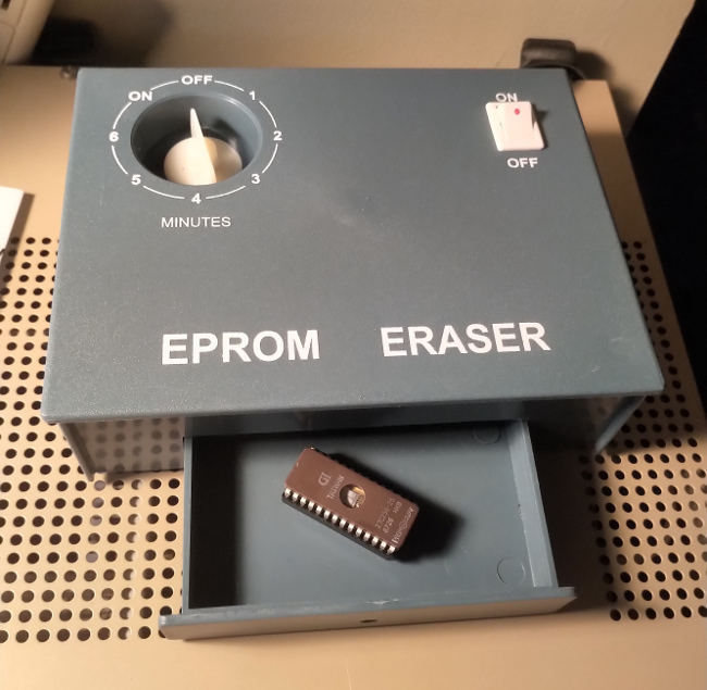
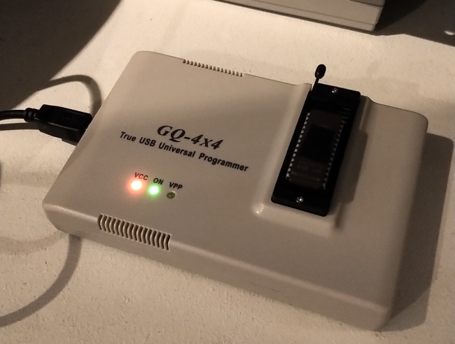
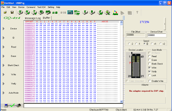
The EPROM required significant investment into an EPROM programmer (or burner - I got MCUmall's GQ-4x4 v4) and an EPROM UV eraser (also from MCUmall). I also ran out of space on my existing breadboards and had to buy several segments.
Running the first program from memory was very satisfying.
Log
day 1Wired up the high 8 bits of the address bus and the 8 bits of the data bus.
All can now be observed via the 16+8 LEDs.
I decided to stick to my current plan of a 74LS244 dedicated to each set of LEDs. This is because even with moderate current, high level voltage output by the 74LS244 that drives the LEDs can drop by 0.2V. I want this to be isolated away from the buses.
Basically, I'd rather add components than have surprises later with the memory, etc., because of inadequate high level voltages.
day 2
Wired up all unused inputs into the ICs used for manual reset and clock.
day 3
Wired up the buffered control lines (CPU outputs).
At this point all control, address, and data lines can be observed via LEDs.
day 4
I am getting ready to connect a ROM to the existing circuit.
First, I had to clean up some breadboard room. It's getting quite busy and I was running out of room on my desk.
I'm going to be using a 27C256-25 EPROM. This is a 256kbit (32kbyte) UV-erasable EPROM.
A few weeks ago I purchased a MCUmall GQ-4x4 EPROM programmer as well as a UV eraser tool, in anticipation for this stage.
day 5
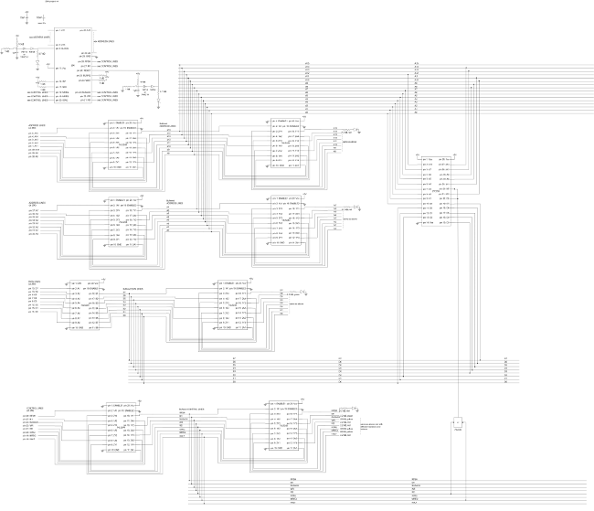
Added the ROM and its connections to the diagram.
Allocated a new breadboard piece for the ROM.
Since there's no RAM (thus no writing to memory) yet, I chose the simplest way to wire up the ROM, combining Z80's MREQ and RD lines through a 72LS32 OR gate, outputting to 27C256's CS and OE lines.
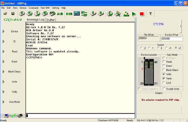
Installed drivers for the EPROM burner inside a Windows XP 32bit virtual machine.
First burn was of a 32k buffer containing only 0x14, which translates to INC D.
Hooked it up and the data bus LEDs are showing an incorrect value.
Instead of 00010100b, it's showing 00101000b, which translates to a conditional relative jump.
This explains why the PC seems to be jumping around randomly, instead of a steady increment as a result of executing the one-byte INC D.
Tried with 0xC3 (11000011b) which worked fine - probably because it's palindromic.
Something is wired backwards.
day 6
Although the data bus LEDs show D7 at the top (consistently with A15, A7 at the top of their LED groups), the data bus itself is wired backwards, with D7 at the bottom.
Rewired the ROM chip and labelled the two inconsistent D7s. This wasn't easy - the breadboard is spaghetti.
I came up with a nice way to protect the pins of the ROM chip. I keep it always inserted into a 28-pin DIP socket, even when I erase it in the EPROM eraser. On the breadboard, the DIP socket is plugged into a pair of pin header strips to stabilize it on the breadboard. This way, the ROM pins are static.
First program:
Address   Bytes        Mnemonic


0000:     00           NOP

0001:     00           NOP

0002:     C3 06 00     JP 0x0006

0005:     00           NOP

0006:     14           INC D

0007:     C3 00 00     JP 0x0000
First attempt at running it failed. It incorrectly read a 0xFF at address 0002.
I checked in the EPROM burner and it's read successfully.
Fixed wire-ups: A0-A3 were wired incorrectly as A3-A0 at LEDs
Fixed wire-ups: A0-A3 were wired incorrectly as A3-A0 at address bus
These two "wrongs" made the "right" of the LEDs displaying expected addresses, despite them being wrong on the bus (and consequently at the ROM).
day 7
I'm testing and still having at least two data lines wired incorrectly somewhere.
Fixed wire-ups: swapped O2 and O5 at ROM.
First program executed successfully from ROM, for the first time!
Z80 diagrams
Here are some useful diagrams, including the Z80 pinout, timing diagrams, etc.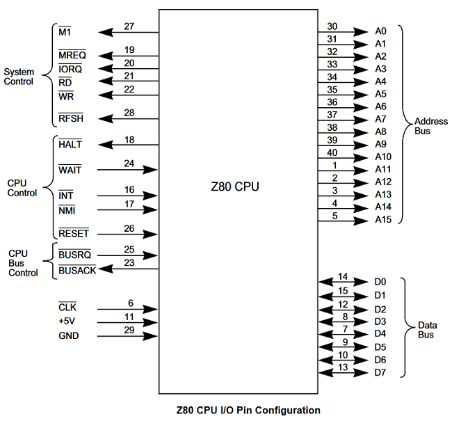

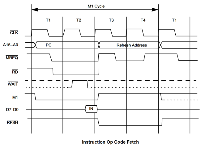


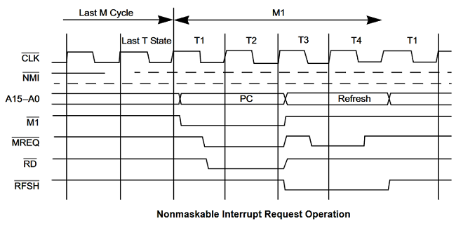


27C256 EPROM diagrams
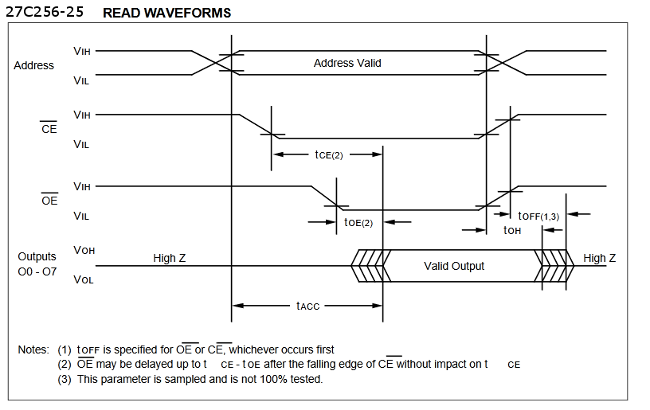
Here are some useful diagrams, including pinout, timing, etc.