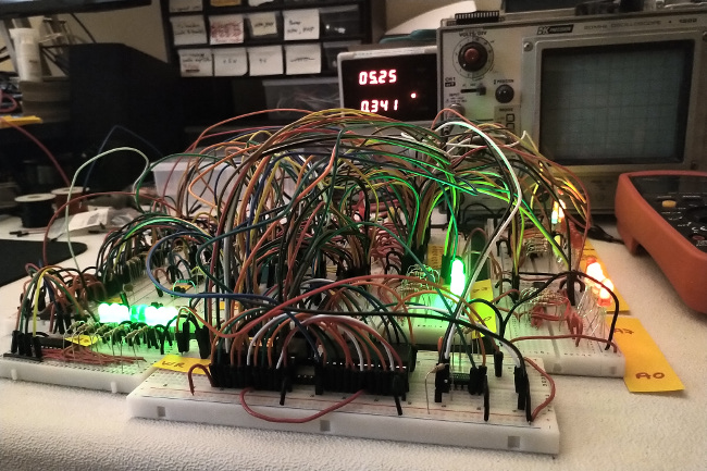
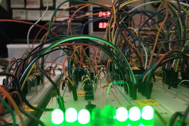
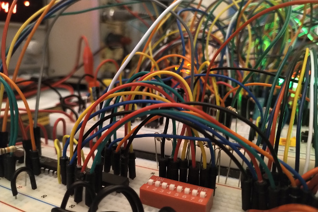
 seb80 - my custom computer based on the Z80 CPU
In this section I've tracked the progression of seb80, from the breadboard prototype, up to the most recent incarnation.
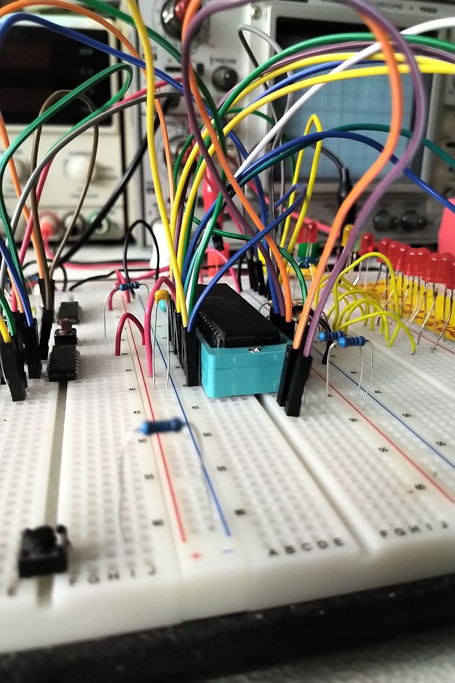
It started with a simple hardwired setup around the Z80 processor, which kept growing in scope, to a computer with RAM and ROM, and which could interface with external devices, through the ROM code I wrote.
This time I've opted to change to LCD1602's 4-bit interface, so that I could wire it up to a single I/O port. Aside from the 4 data lines, 2 additionsal lines are used for REGSEL (register select) and ENABLE.
This involved some code changes from the code I wrote back when I interfaced the LCD with Snowdrop OS, on top of the port from x86 to Z80 assembly language.
ROM version 1 binary
ROM version 1 source
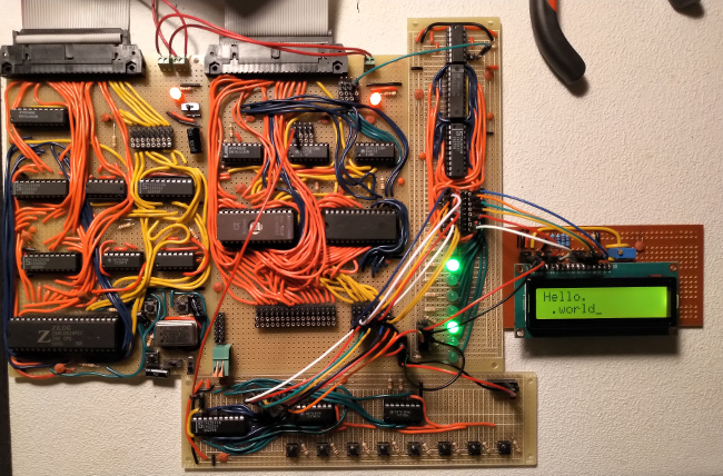
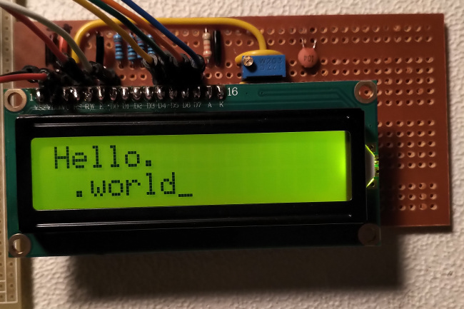
Refreshed memory of how to interface a LCD 16x2.
I realized that if I restrict the set of characters I can display on the LCD, I can use only 6 data lines, reserving 2 for control (ENABLE and REGSEL-register select).
Looking at digits 0 through 9 and letters a through z:
it is clear that to display all of these, LCD's D7 can be hardwired low and D5 can be hardwired high.
This means that CPU's D7 can be used for ENABLE and D5 for REGSEL.
day 2
Yesterday's plan won't work. During initialization, the LCD controller needs multiple data lines including D7 and D5. This means that I cannot simply hardwire them.
The bad news is that a second latch is needed. The good news is that the entire ASCII character set will be available.
Spent one hour troubleshooting why output to the LCD was garbled and unstable.
The issue was that the latch IC (74LS373) was missing its connection between pin 1 (OUTPUT) and ground.
seb80 can now write to a simple display! This was accomplished by porting my x86 LCD code to Z80.
day 3
I'm going to try using the LCD controller in 4-bit mode. It's somewhat more complex, but it would save me components.
Converted the driver code to use 4-bit mode, eliminating a few ICs and an output device port.
day 4
Soldered everything needed for the display.
Found out the hard way that machined male pin headers make poor contact with regular female pin headers.
This required desoldering of the LCD's machined pin headers, replacing them with regular ones.
Fixed an issue whereby the 10 kOhm resistor I used to bring R/W low was causing the LCD to no longer initialize. The solution was to hardwire R/W directly to ground.
day 5
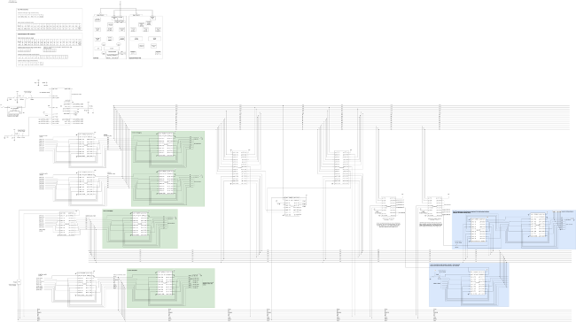
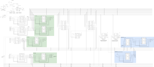
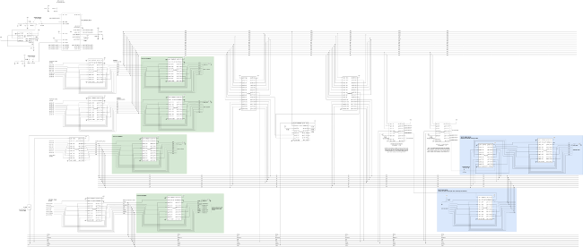
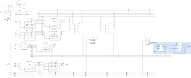
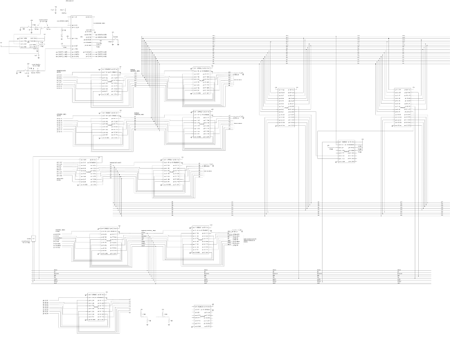
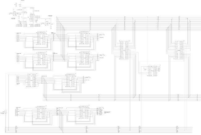
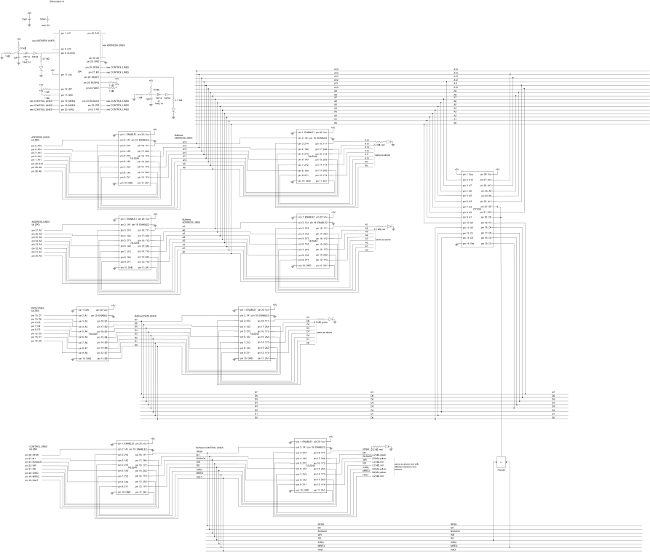
Updated diagram.
day 6
Started work on ROM updates, around keyboard and display functionality.
day 7
Wrote a scan code to ASCII conversion routine.
day 8
Wrote functionality for reading user input into a buffer.
All ICs are placed in sockets, to make it easy to replace if they get damaged. I've used higher-quality machined sockets for those which might be replaced more routinely: the ROM and the oscillator.
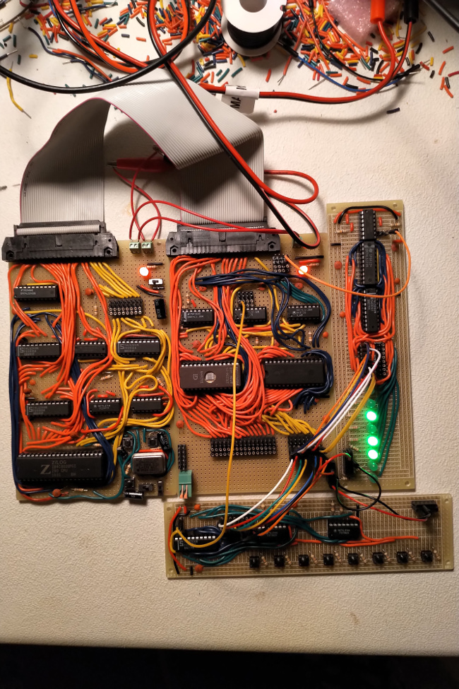
The computer proper is made up of two boards: CPU board and memory/expansion board. The computer also has built-in 4 input device selectors and 4 output device selectors, to reduce the amount of external circuitry needed for these first 8 devices.
I've built two simple devices on their own PCBs. One is a latch/interface board. It latches data written to it via OUT instructions, making it available to a consumer device via a set of pin headers. Eight on-board LEDs display this latched data, which makes the board useful for debugging, as well.
The second device is a minimalistic keyboard, which uses 8 push buttons. 7 bits are available to compose a "key", while the last button is used as a latch. ROM software reads in the 7 bits only when the latch bit goes high (is pressed).
At this time, its ROM (version 0) simply writes to the output device whenever a value is latched by the user on the keyboard.
ROM version 0 binary
ROM version 0 source
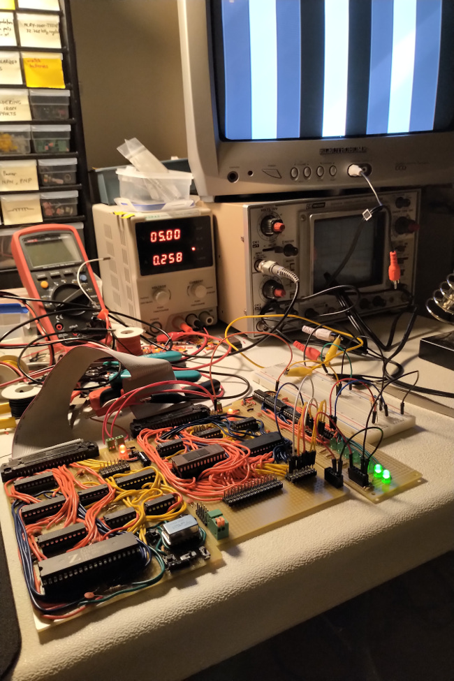
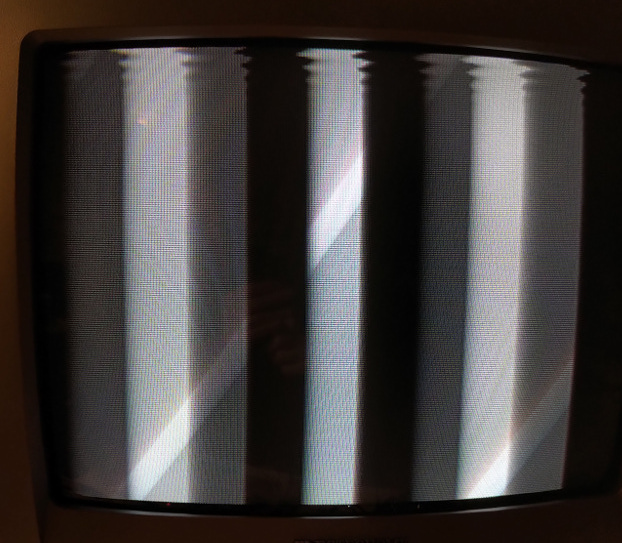
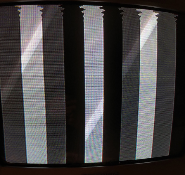 With low capacitance at the output, transitions between stripes are noisy.
 Transitions improve with a 10 nF capacitor at the output.
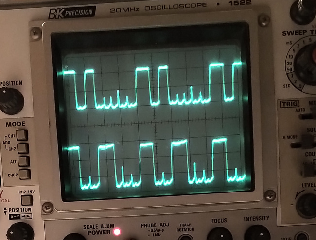 Crosstalk in wires when using a 3.6864 MHz clock: the taller spikes reach 2 V, sometimes disturbing the circuit enough to cause faults - possibly because low level noise moves signal up into TTL high level voltages (around 2 V).
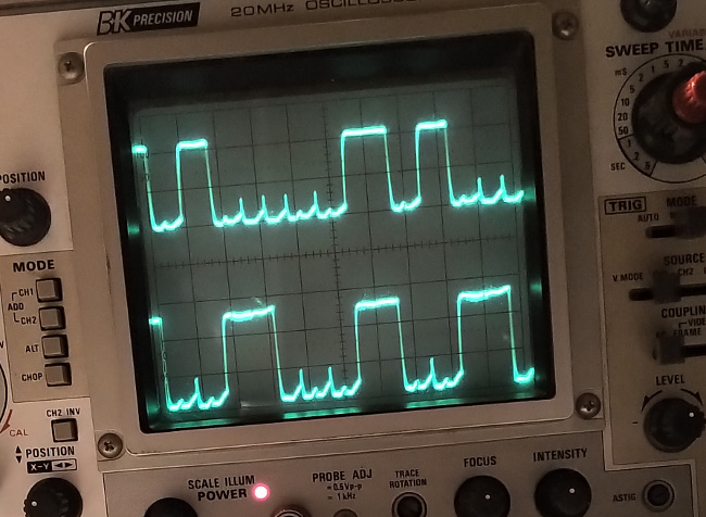 Switching to a 2.4576 MHz clock eliminates the taller spikes. Noise still exists, but is no more than 1 V - not enough to cross into TTL high level voltage range.
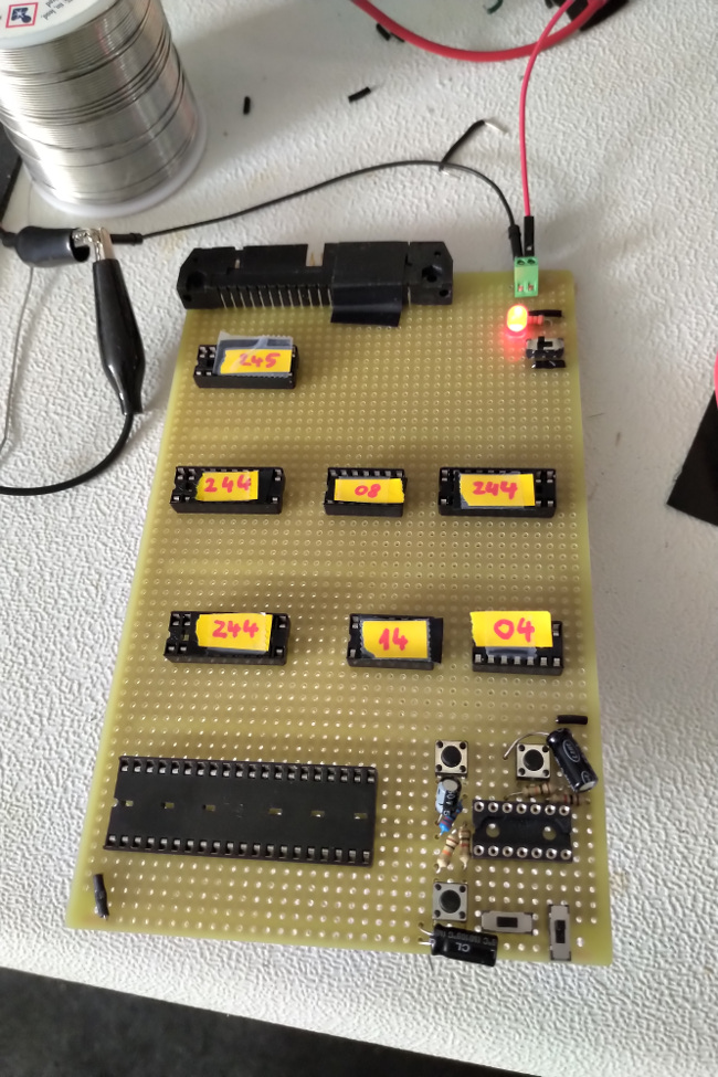
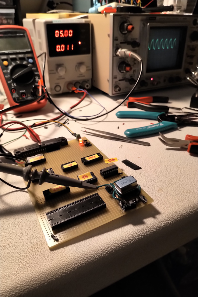 A first heartbeat.
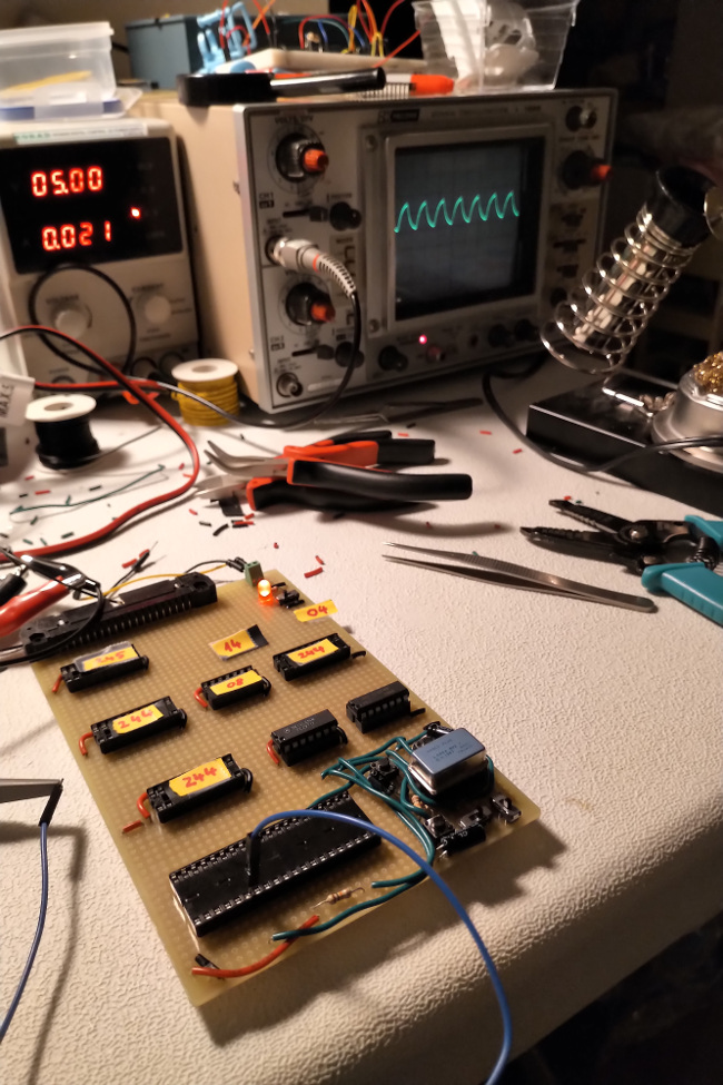
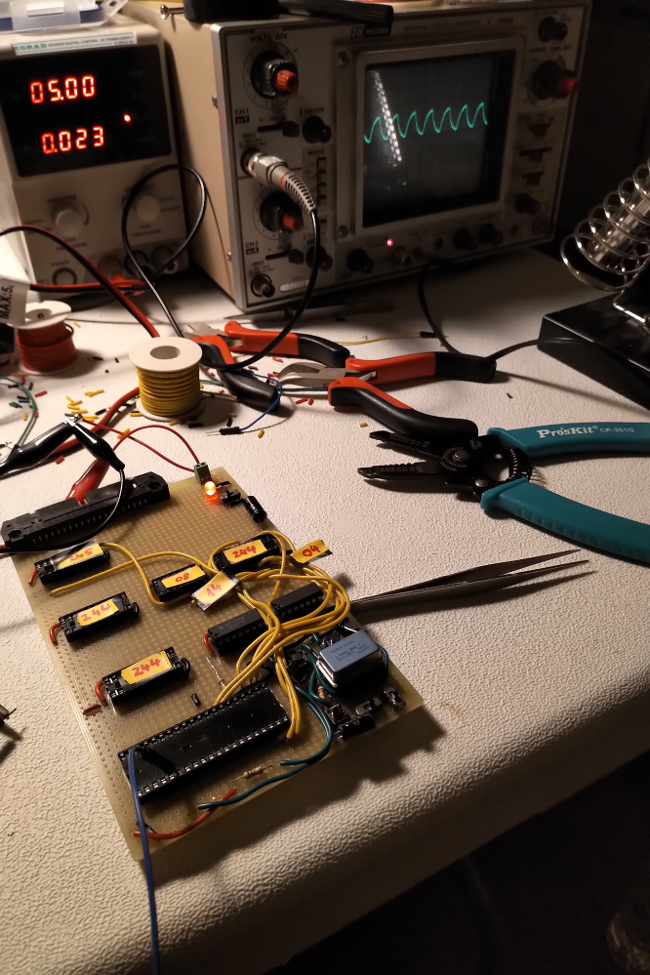
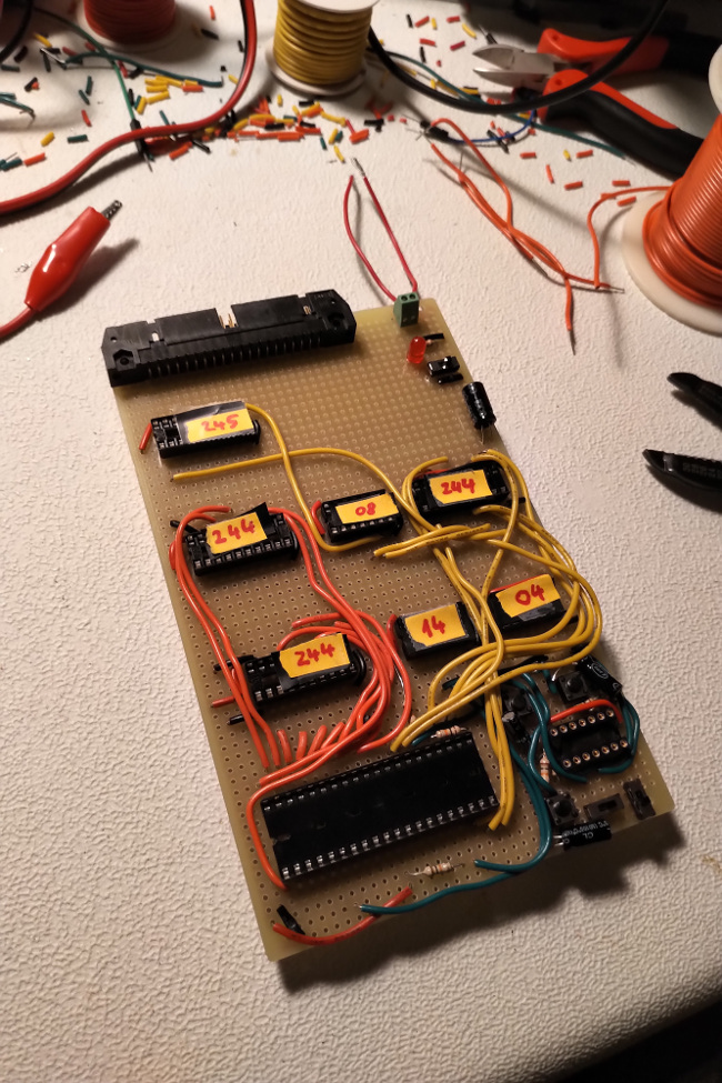
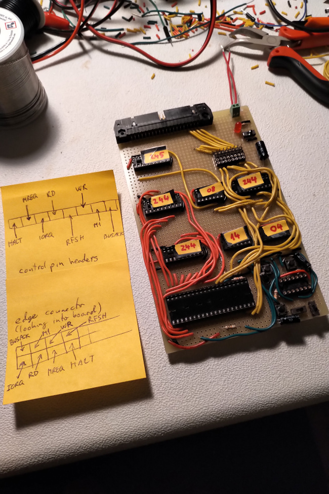
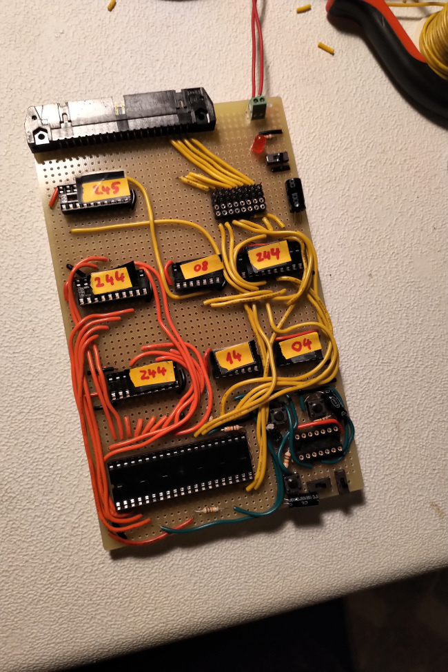
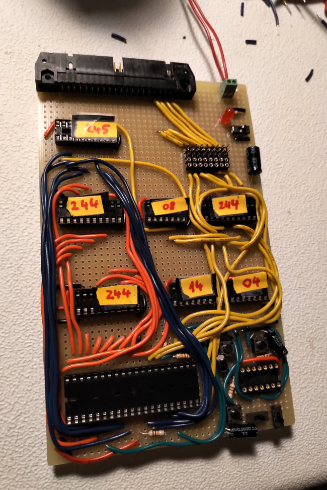
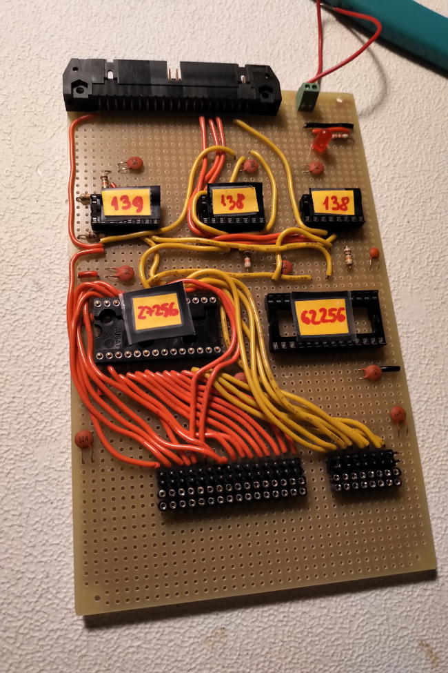
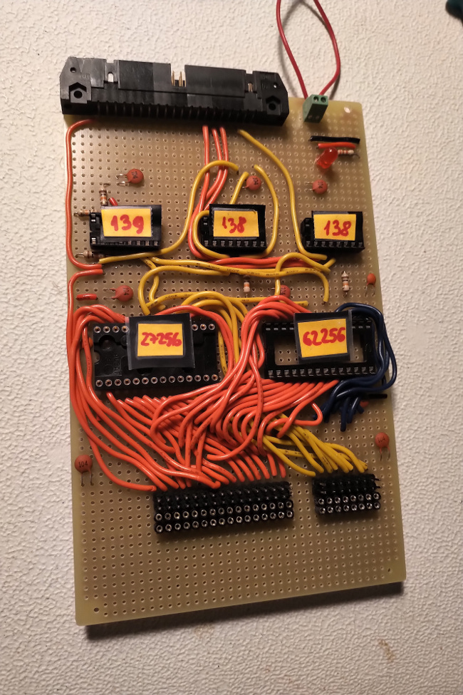
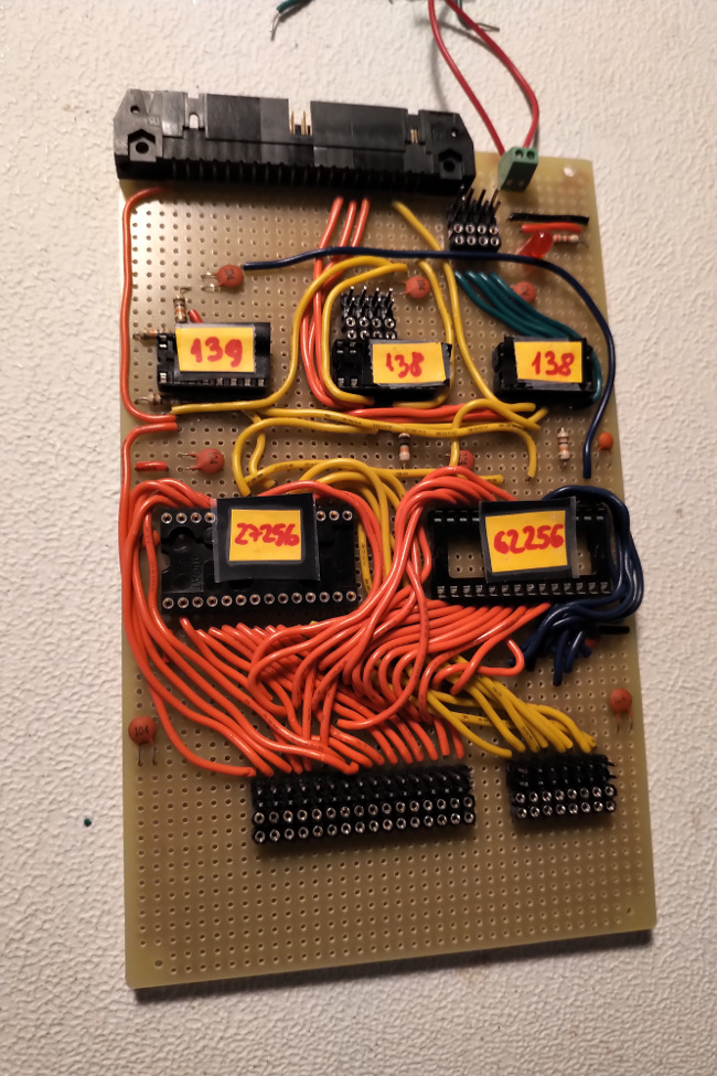
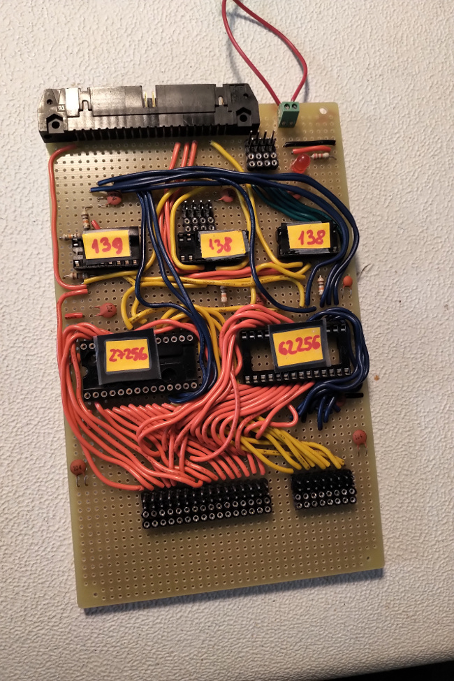
 IC socket pins are very sharp.
The crystal oscillator needs its own power switch, or it freezes the CPU, even if not connected to the clock pin.
Started designing the CPU PCB.
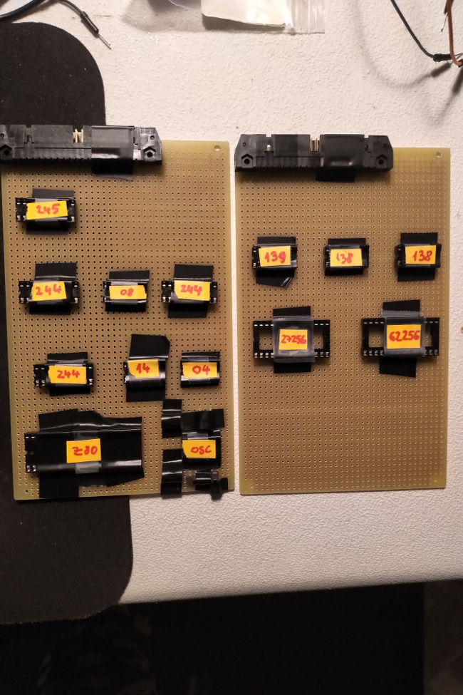
I'm using electrical tape to fix IC sockets and switches onto the PCB first.
I've started with the CPU and clock.
day 2
Work continues on planning the layout of the CPU PCB.
I've decided to use higher-quality (and more expensive) machined sockets for the ICs that will be more often removed and re-inserted (such as EPROM and oscillator).
day 3
The layout is mostly decided on and soldering has begun.
I'm starting with the CPU board, which is the more difficult one - due to the multitude of connections.
I've started with the clock, reset, and NMI circuits.
day 4
Soldering continues.
The clock, reset, and NMI circuits are all connected to the 40-pin Z80 socket.
Soldered all IC sockets entirely.
Also soldered edge connector entirely. It was difficult due to everything being so close together and having to jump traces.
Burned my fingers twice and stabbed one deeply enough to bleed.
day 5
More soldering, moved on to CPU's control lines.
day 6
More soldering, moved on to CPU's address lines.
day 7
More soldering, the CPU control (output) lines are now connected all the way to the edge connector.
I have decided to bring the pin headers (for external connections) onto the CPU board, since it was not only convenient, but I had some spare room on it.
This also reduces the amount of wires running across the secondary (memory/extension) board by 20-25%.
day 8
More soldering, moved on to CPU's data lines.
day 9
More soldering, moved on to bringing the address lines to the edge connector.
day 10
With the addition of a few bypass capacitors, the CPU board is complete for now.
I'm moving on to the memory/expansion board.
Soldered the edge connector and all IC sockets on the memory/expansion board.
day 11
Another day of soldering, another bloody finger.
Started with all bypass capacitors, since I think it's easier to add them first, to run all wires on top of them, as they lay flat.
Moved on to memory chip and I/O device selectors.
Soldered all inputs to the selectors, as well as all control lines for RAM and ROM.
day 12
Updated diagram with PCB details (connectors, etc.)
Started preparing all pin headers for the expansion points (2 male and 2 female pins for each address line, data line, 4 input devices, 4 output devices).
day 13
Finished preparation of pin headers; I now have all necessary segments.
Soldered address and data expansion pin headers. It was stressful, since there was such a high density of connections.
Soldered ROM to expansion.
The plan is to solder RAM to expansion, and then ROM to edge connector.
day 14
Ceramic disc capacitors have very sharp pins. I found this out while getting another bloody finger.
Soldered RAM to expansion.
Soldered the 4 input device selectors and 4 output device selectors.
Added all connectors to diagram.
day 15
Soldered RAM and ROM to edge connector, which connects all components to the address and data buses.
Added a few power connectors for any external devices to be supplied easily.
Added a PCB layout diagram to the overall diagram.
day 16
These IC sockets are strong. The RAM one gave me 5 inline stabs while trying to pry the IC out of it.
The time I spent carefully checking all connections has paid off: the computer worked "out of the box"!
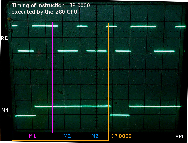
My first test was with a simple infinite loop at address 0: JP 0
I was able to match the M1/RD timing I observed on the oscilloscope, with one I recorded earlier.
The one from before used a 0.1 MHz clock; its edges were clean, and its high/low levels stable.
This one uses a 3.63 MHz clock; its edges are clearly affected by stray capacitance. Its high/low levels are impacted by - most likely - crosstalk in the ribbon cable, showing as much as a 0.5 V fluctuation in what should be constant high level voltage. Low level fluctuation is smaller, at around 0.3 V.
I'm glad the TTL standard has enough slack built in.
New issue: IORQ, WR seem to not output correctly, staying high past the 74LS244 buffer. This causes the I/O output device selector to not function at all.
This took a few hours to troubleshoot, and it was a combination of issues.
First, IORQ and WR did output correctly. It was just impossible to see on the oscilloscope, as the low state lasted such a short time compared to everything else.
Second, latched output was in fact correct, although initially it seemed fast enough to mean that the latch was in its pass-through state at all times. The issue is that I had reused a program which I wrote (and tested) with a significantly slower clock speed (perhaps 1 kHz), whereas now the clock is at 3.6864 MHz. This and the above made it seem like the latch was always pass-through because IORQ and WR stayed high (inactive).
Third, to make things more difficult, I damaged a Z80 - most likely by discharging static electricity into it. The air in the room is quite dry this time of year. I have to be more careful around these CPUs.
Fourth, it seems like channel 2 of my oscilloscope is sometimes malfunctioning. For some reason it won't pick up voltage changes, except at high frequencies.
After a few modifications to the program, I can clearly see IORQ and WR on the oscilloscope as well.
day 17
Brought over the NTSC signal generation circuit and tested it successfully.
Next, I will create a latch device which can be used as a generic output device, based on the 74LS373. Its outputs will be buffered via a 74LS244.
Wasted an IC socket after choosing a cheap PCB whose traces had unintended contacts.
Decided to use a good PCB rather than a cheap one.
day 18
Finished soldering the latch device on a PCB.
This device offers 8-bit data output that is latched when a byte is written to its hardware I/O port.
Any consumer device can rely on this to receive data from the Z80 reliably.
Bonus: because I had room on the board, I also connected 8 LEDs to the outputs. This makes it excellent for debugging - for example, the value of the accumulator can be written to it and then observed by a human.
From the specs, the 74LS244 can source 15 mA from a logical high output pin (more from a logical low). I've measured the green LEDs at 2.3 V and they're in series with 2.2 kOhm. From the 74LS244's measured logical high of 3.2 V, the LEDs consume about 0.4 mA, leaving quite a bit for a low-power device to draw directly from this latch board.
day 19
Started work on the computer's first input device.
It's based on 8 push buttons, each hardware-debounced via a Schmitt trigger.
I expect to use one of the switches as the "latch", so that it's easy to interface this device by polling.
day 20
More soldering on the keyboard.
day 21
Finished soldering the keyboard.
Updated diagram.
day 22
The computer is now officially named seb80 (intentionally all lowercase). It sounds a bit like "zed eighty", the CPU.
Laid the foundation for seb80's ROM.
It will feature a collection of useful routines, including delays, keyboard, etc.
Wrote a keyboard routine which will register latches and return both whether something was just latched and current hardware button state.
This proves that the keyboard module works - and it works the first time!
I am very pleased that for the amount (I approximate around 1000 points) of soldering I have done, everything worked the first time; no soldering fix-ups were needed. Much of that is owed to the time I spent updating and verifying the diagram, as well as on-going continuity testing after each batch of connections I soldered.
day 23
Finished up ROM development for this version.
Anything faster than the 3.6864 MHz crystal oscillator I ultimately chose caused system instability.
Generating stable NTSC frames requires consistent timing. Visible scan lines need to have their horizontal sync pulses at the same time, to prevent image distortion (shearing, rolling, etc.) The number of invisible, vertical sync scan lines varies significantly from TV to TV.
The interfacing circuit is very simple. Given that NTSC televisions have a terminating 75 Ohm resistor at their input, it was simple to design a Y resistor network connected to two pins of an output device. Pin 0 had 1k Ohm and pin 1 had 470 Ohm. Approximately, 00b output 0V (sync), 01b output 0.3V (black), 10b output 0.7V (gray), 11b output 1V (white).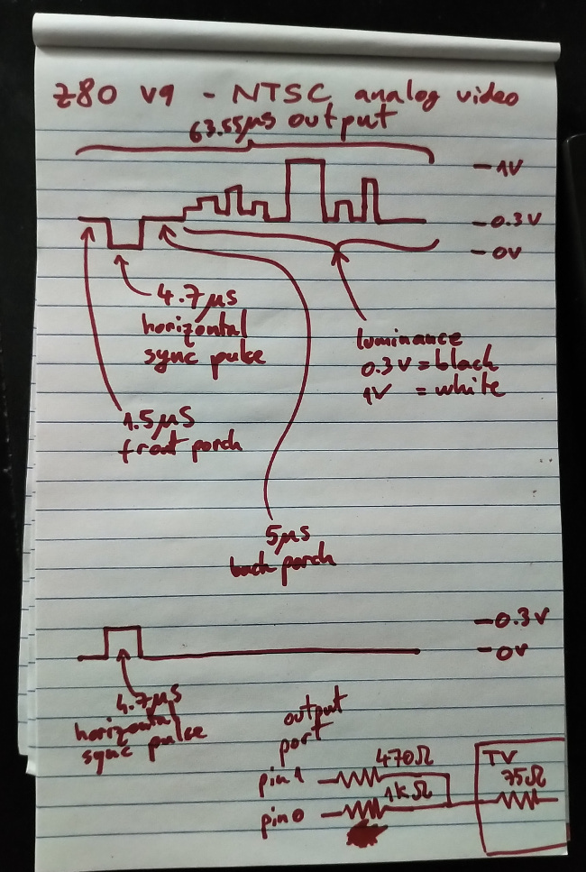
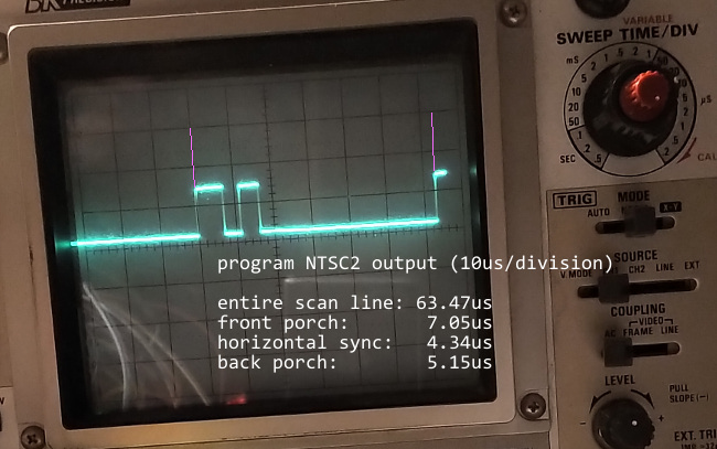
I've used program NTSC2 to get consistent scan line timing, before setting out to display anything on a television set yet.
Programs NTSC4 and NTSC5 below are complete examples of generating static images, as well as dynamic images, based on modifications made by a user via an input.
NTSC4 program - generates a static image
NTSC5 program - generates a vertical bar which can be moved with a button
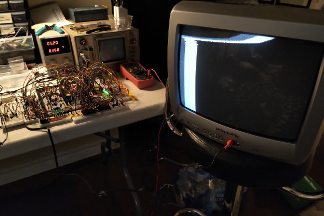
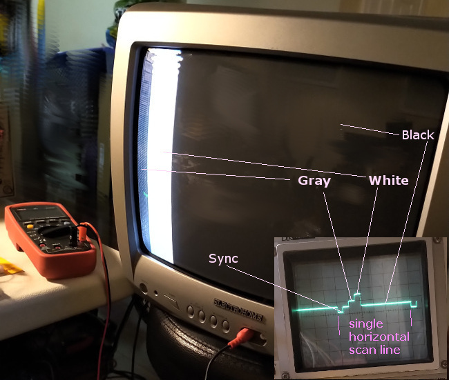
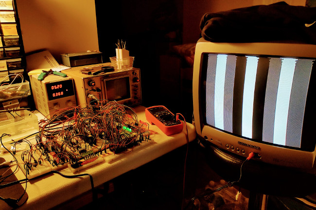
Bought a 3.6864 MHz oscillator crystal metal package. Period is 0.271267361us.
I first had to figure out the pinout, since the only data sheet I found for this RASCO PLUS oscillator was unclear which pin was which.
I was happy to see that the computer runs well at a frequency into the megahertz, since so far the fastest I've run it was around 1 kHz.
This is because I have so many long wires everywhere on the breadboard, that I thought stray capacitance would add enough noise for the CPU to be unstable.
One thing I'm noticing is that the CPU freezes if I try to clock it manually while the oscillator is active (though not inputting into the CPU's clock pin).
I found a way to work around this: power off the oscillator and the manual clock will work fine.
day 2
My plan is to re-visit a project from university.
While most of courses in university were computer science (theory, programming, etc.), one of the most enjoyable was ECE385H: Microprocessor Systems. It was a lab-heavy course in which we interfaced various components together.
One of the lab projects involved using an Atmel microcontroller to generate timing accurate enough to create a steady image on a television screen. The circuitry needed was minimal: a purpose-built resistor network acting as a DAC to input into a television set's analog coaxial input.
The driver program was written in C and the timing of our program (when to write various values to an output port) had to respect the NTSC standard closely enough to generate a black-and-white image.
This is what I wish to re-create here - this time not using a microcontroller and C, but using my own custom Z80 computer.
This time, I think that I'll have the extra advantage of more precise timings for my loops, etc., due to writing the driver program in Z80 assembly language - thus having the benefit of knowing exactly how many clocks (T-states) each instruction will take.
day 3
Began timing planning.
Each NTSC video frame draws 242 visible scan lines and 20 invisible scan lines ("vertical blanking").
NOTE: Since front and back porches are at black-level voltage (0.3V), I can extend their durations, to be a bit safer.
The cost of this is reduced horizontal resolution (since some of the left and right edges will always be black), which I accept.
My main concern (looking at these timings) is to generate a short and accurate horizontal sync pulse - since that's the shortest transition of all durations.
If the 0V level is represented by logical 0, then I can have the 0.3V level be represented by logical 1.
The following is my first timing prototype for repeatedly generating scan lines.
This is meant to be observed on an oscilloscope, since it has no vertical blanking interval - just hardcoded scan lines.
day 4
First attempt at scan line timing was promising: entire scan line is about 0.55us short, front porch and back porch are about 5us too long.
I have also tried running this breadboard computer from a 10 MHz crystal oscillator and it was unstable, so I abandoned it for now.
It will probably work well once I build the computer on PCBs, but there's just too much interference on the breadboards (long wires, etc.)
Found a suitable command-line assembler. The programs are becoming too large to type in hex values by hand.
day 5
Spent some more time adjusting the visible scan line loop.
Converted the program from an infinite loop to a finite one, performing 242 iterations - one for each visible scan line.
Added the vertical blanking interval line loop. This is where calculations and changing memory will take place, so that the visible scan line loop is as fast as possible.
Added a CMOS inverter to get output voltages closer to supply and 0.
Hooked up to a television (resistor values 1000Ohm on pin 0 and 470Ohm on pin 1) and I'm seeing an image for the first time!
Problems: top of the screen is sheared and gray-coloured bar looks black.
Removed the CMOS inverter and used the TTL outputs of the 74LS244 buffer directly. This made the gray bar visible!
At this point, something is not synchronizing properly, and I believe it's the vertical.
I don't think it's the horizontal because the lines that are NOT sheared are output by the exact same loop and look fine.
Reduced the vertical blanking line count from 20 to 10. Sheared region is smaller.
Reduced the vertical blanking line count from 10 to 5. Sheared region is smaller.
day 6
Reduced the vertical blanking line count from 5 to 2. Sheared region is smaller.
For displaying vertical bars, I found that using OUTI and re-initializing HL to point to the start of a colour array is the fastest.
The image is static and stable. The program which generates it is called NTSC4.
day 7
Started work on a program that updates something on the screen when an input device changes state.
day 8
Finished NTSC5, the program which moves a vertical line on screen whenever a button is pressed.
The input device I built is a segment of 8 DIP switches.
TP6 - test program for I/O input
This begins part 2 of interfacing with I/O devices; in this version I want to add the necessary circuitry to be able to input from devices.
Just like for output devices, a 74LS138 3-to-8 decoder (part is SN74LS138N) will be used to enable one of up to four input devices.
Already, I/O devices at port 4, 5, 6, 7 (A2=1) are be output devices.
Thus, I/O devices at port 0, 1, 2, 3 (A2=0) will be input devices.
NOTE: for input devices that won't rely on these built-in selectors, care has to be taken that they are wired to ports whose A2=1, to not conflict with the built-in input device selectors which expect A2=0.
day 2
The second 74LS138 was easy to design; it's just like the output one, except being enabled by Z80's RD line (along with IORQ).
The switches will be buffered by a 74LS244, enabled by one of the input device selector's outputs.
day 3
Wired up the input selector 74LS138.
Wrote TP6, a test program to test input via a device made up of switches:
Verified that the 74LS138 correctly selects an input device, as wired.
Wired up the 74LS244. It was much easier than before, with the extensive wiring diagram I've been maintaining.
Program TP6 ran successfully, demonstrating the full I/O cycle (read from DIP switches, write to LEDs).
The device's entry point is a 74LS373 octal d-type latch which snapshots the data bus when enabled. It is enabled by one of the outputs of a 74LS138 3-to-8 decoder, which serves as an output device selector.
The latch output is buffered by a 74LS244, which provides sufficient current for the LEDs.
See the log below for program listings.
TP4 - test program for I/O output
TP5 - increment-and-output test program for I/O
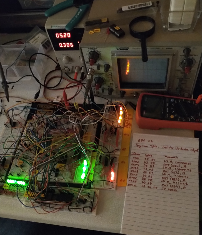
Began designing the I/O circuit. My plan is to expose selectors for eight different I/O devices via a 74LS138 3-to-8 decoder (part is SN74LS138N).
Wiring this up to A0-A2 will allow easy access to I/O ports 0 through 7.
For the prototyping stage (on the breadboard), I want to wire up and output device made up of 8 LEDs which will display the last value written to the respective I/O port.
I realized that by adding a second 74LS138 3-to-8 decoder I could expose 4 input and 4 output devices with no further chips.
One 74LS138 will rely on Z80's RD line to become enabled and the other will rely on Z80's WR line to become enabled.
Address line A2 will select between the first 4 and the next 4.
I/O devices at port 0, 1, 2, 3 (A2=0) will be input devices.
I/O devices at port 4, 5, 6, 7 (A2=1) will be output devices.
NOTE: for input devices that won't rely on these built-in selectors, care has to be taken that they are wired to ports whose A2=1, to not conflict with the built-in input device selectors which expect A2=0.
Output devices:
day 2
Wired the 74LS138 which will select between four output devices.
Wrote TP4, my first I/O output test program.
Verified with a multimeter that the output device selector (74LS138) works as intended.
Since the main breadboard is running out of room, I've brought out the data lines onto a side breadboard.
Designed the first output device: 8 LEDs.
It's based on 74LS373 (part is DM74LS373N) octal d-type latch (transparent). While this latch has the advantage of having a level-sensitive LE (latch enable), it is active high, unlike all other TTL chips I've used so far. Luckily, my 74LS04 hex inverter still has some free slots.
The I/O output device selector was already tested, so all I had to do is connect a small breadboard which already had LEDs and a 74LS244 buffer wired up.
Wrote program TP5, below, which is supposed to successively write higher values to an output device, with visible delay. NMI should reset the value to 0.
The program ran successfully! The counter was observable on the LEDs of the output device and NMI successfully reset the counter to zero.
day 4
Updated diagram
See the log below for program listings.
TP1 - test program for NMI
TP2 - test program for INT
TP3 - second test program for NMI
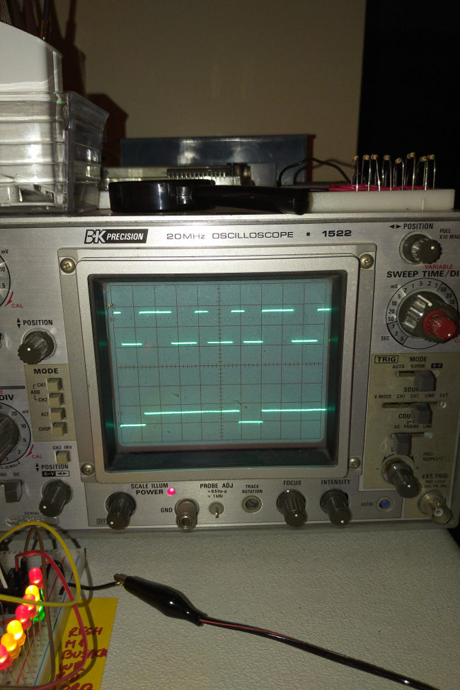
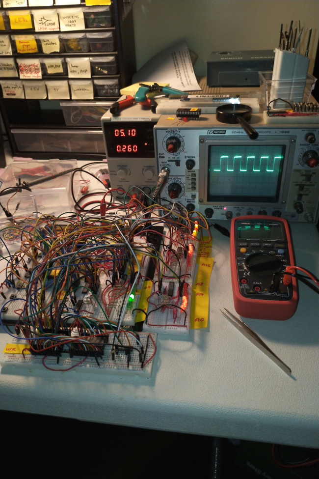
Wired up a 555 circuit.
I did it much faster than the last time I worked with a 555, probably because of the few hundred connections I've made for the Z80.
day 2
Replaced the last two 74F series chips with 74LS, to rely exclusively on the 74LS family of TTL logic ICs.
Broke a pin on one CPU and discovered that another one was faulty (internal short-circuit).
That means I'm down to two good CPUs.
Re-wired the manual clock ICs and introduced a switch which selects between manual clock and 555-driven clock.
This has allowed me for the first time to observe instruction timing on an oscilloscope.
day 3
Reset is now automatic. I used a simple RC circuit to make the RESET pin start low at power-on and reach 2V after a generous 0.8 seconds - giving enough low-level time for three clocks, ensuring a successful reset.
It will also feature a push button to allow manual reset as well, for the cases when clock is manual or just to reset more easily partway through program execution.
day 4
Designed a "generate NMI" button. I debounced it just like the clock button, to prevent multiple NMIs from being generated on a push.
Wrote TP1, the NMI test program.
Program was verified successfully! Before NMI is generated, the CPU loops between 0008 and 000D. After NMI is generated, the CPU enters the infinite loop at 0010.
day 5
Changed all pull-up resistors in my design to 10k for consistency's sake.
I'm going to test INT interrupt signals with a bouncy push button. For fun, I will be able to see how many bounces each push generated.
Wrote TP2, the INT test program.
Verified that the counter is incremented when an interrupt signal is raised.
Made a second test program for NMI, to count invocations.
Successfully observed NMI incrementing the counter variable.
This maps memory addresses 0000-7FFF to ROM and 8000-FFFF to RAM.
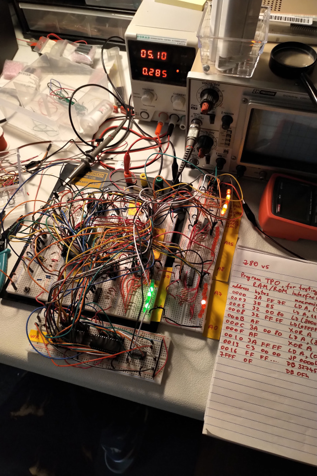
To test my new setup, I've written a program which reads and writes (to RAM only) to the edges of RAM and ROM. I've asserted that the setup was valid by observing the data line LEDs as the Z80 read values from memory - and then comparing to my expectation.
See the log below for the program listing. You can also download the 32kb ROM binary here.
Validated my expectation that for IO writes, the Z80 keeps correct write data on its data lines past IORQ/WR returning to their inactive state.
This means that interfacing with D-type flip-flops should be reasonably easy.
My plan is to use them for a built-in, write-only device made up of 8 LEDs which I'll use for debugging, by simply OUTputting byte values (which get latched) to it.
day 2
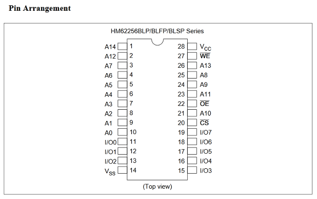
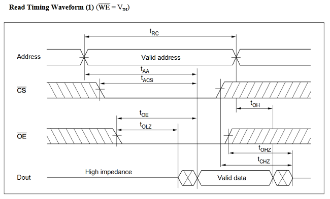
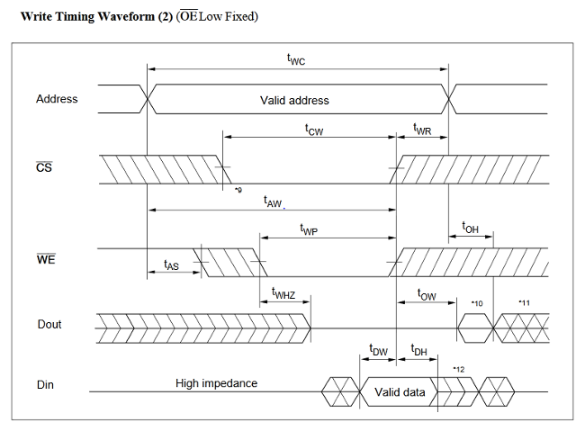
Started planning and diagramming the integration of the RAM chip. I'm using a Hitachi HM62256LP-70.
This is nice: the HM62256's pinout is very similar to the 27C256's.
By placing the RAM chip next to the ROM chip on the breadboard, I was able to bring address and data to the RAM chip neatly, using some very short jumper wires.
The RAM chip is fully wired up except for its control lines, which I still have to design.
I've hardwired its control (CS, OE, WE) high (inactive), so that I can still test that the ROM works well.
day 3
Designed final connections of data bus transceiver (74LS245) and settled on a chip select strategy.
Wired the 74LS245 transceiver to be enabled and disabled by the Z80, depending on MREQ and IORQ (when either becomes active). This was done simply with a 74LS08 AND gate.
Wired the 74LS245 transceiver to have its direction controlled by the Z80 via direct connection to Z80's RD line.
This many breadboards are dropping some voltage, so I've increase supply to 5.1V.
day 4
Designed the memory chip selection circuit. It will simply split on A15 between a 32k RAM chip and a 32k ROM chip.
This way all memory registers are uniquely addressable and all memory registers are addressable
For both RAM and ROM, OE (output enable) lines are connected directly to the RD line on the bus.
For RAM, WE (write enable) line is connected directly to the WR line on the bus.
To select one of RAM and ROM, I've used a 74LS139 1-of-4 decoder (also called 2-to-4). The exact part is DM74LS139.
The 74LS139 is enabled by Z80's MREQ. Its A input is tied to Z80's A15. Its B input is hardwired high.
day 5
Wired everything, moving previous connections to the ROM onto the decoder.
Ran the program below successfully, verifying reading from end of ROM, as well as writing and then reading from beginning and end of RAM:
Assertions were done via the LD a, (MMMM) statements, where I verified that the data lines contained the proper byte that was expected to exist in memory at the specified address. I also measured the output of the decoder to verify that it was activating the expected memory chip each time.
day 6
Brought diagram up to date.
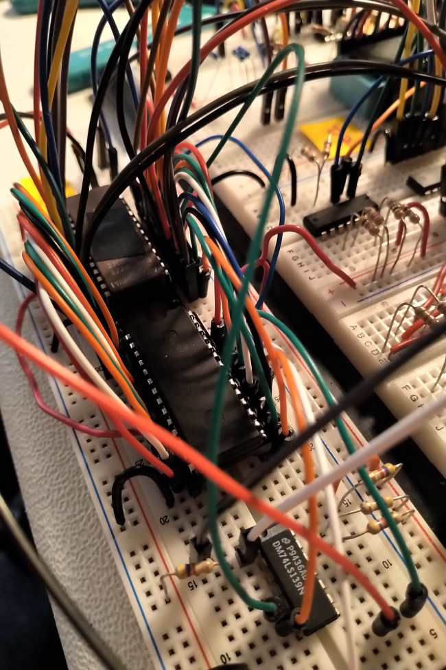
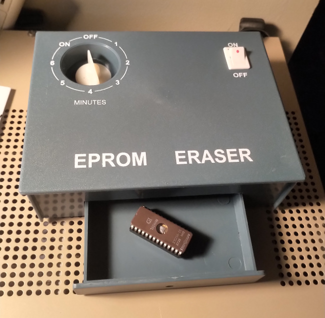
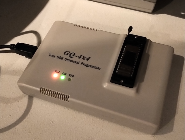
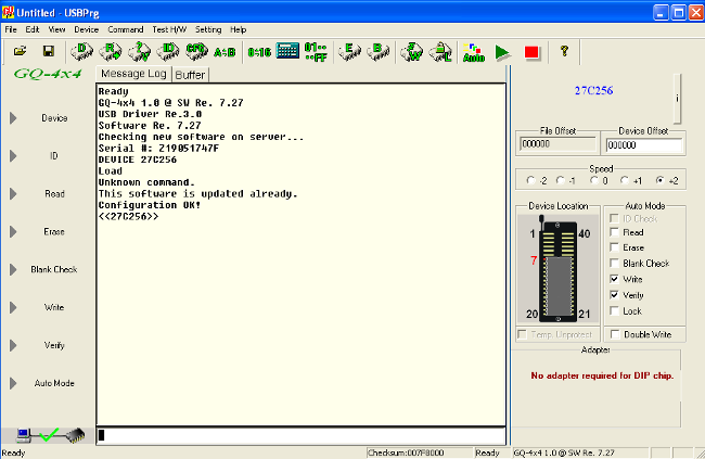
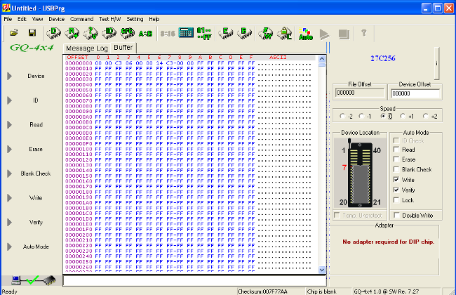
The EPROM required significant investment into an EPROM programmer (or burner - I got MCUmall's GQ-4x4 v4) and an EPROM UV eraser (also from MCUmall). I also ran out of space on my existing breadboards and had to buy several segments.
Running the first program from memory was very satisfying.
Wired up the high 8 bits of the address bus and the 8 bits of the data bus.
All can now be observed via the 16+8 LEDs.
I decided to stick to my current plan of a 74LS244 dedicated to each set of LEDs. This is because even with moderate current, high level voltage output by the 74LS244 that drives the LEDs can drop by 0.2V. I want this to be isolated away from the buses.
Basically, I'd rather add components than have surprises later with the memory, etc., because of inadequate high level voltages.
day 2
Wired up all unused inputs into the ICs used for manual reset and clock.
day 3
Wired up the buffered control lines (CPU outputs).
At this point all control, address, and data lines can be observed via LEDs.
day 4
I am getting ready to connect a ROM to the existing circuit.
First, I had to clean up some breadboard room. It's getting quite busy and I was running out of room on my desk.
I'm going to be using a 27C256-25 EPROM. This is a 256kbit (32kbyte) UV-erasable EPROM.
A few weeks ago I purchased a MCUmall GQ-4x4 EPROM programmer as well as a UV eraser tool, in anticipation for this stage.
day 5
Added the ROM and its connections to the diagram.
Allocated a new breadboard piece for the ROM.
Since there's no RAM (thus no writing to memory) yet, I chose the simplest way to wire up the ROM, combining Z80's MREQ and RD lines through a 72LS32 OR gate, outputting to 27C256's CS and OE lines.
Installed drivers for the EPROM burner inside a Windows XP 32bit virtual machine.
First burn was of a 32k buffer containing only 0x14, which translates to INC D.
Hooked it up and the data bus LEDs are showing an incorrect value.
Instead of 00010100b, it's showing 00101000b, which translates to a conditional relative jump.
This explains why the PC seems to be jumping around randomly, instead of a steady increment as a result of executing the one-byte INC D.
Tried with 0xC3 (11000011b) which worked fine - probably because it's palindromic.
Something is wired backwards.
day 6
Although the data bus LEDs show D7 at the top (consistently with A15, A7 at the top of their LED groups), the data bus itself is wired backwards, with D7 at the bottom.
Rewired the ROM chip and labelled the two inconsistent D7s. This wasn't easy - the breadboard is spaghetti.
I came up with a nice way to protect the pins of the ROM chip. I keep it always inserted into a 28-pin DIP socket, even when I erase it in the EPROM eraser. On the breadboard, the DIP socket is plugged into a pair of pin header strips to stabilize it on the breadboard. This way, the ROM pins are static.
First program:
First attempt at running it failed. It incorrectly read a 0xFF at address 0002.
I checked in the EPROM burner and it's read successfully.
Fixed wire-ups: A0-A3 were wired incorrectly as A3-A0 at LEDs
Fixed wire-ups: A0-A3 were wired incorrectly as A3-A0 at address bus
These two "wrongs" made the "right" of the LEDs displaying expected addresses, despite them being wrong on the bus (and consequently at the ROM).
day 7
I'm testing and still having at least two data lines wired incorrectly somewhere.
Fixed wire-ups: swapped O2 and O5 at ROM.
First program executed successfully from ROM, for the first time!
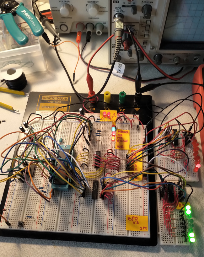
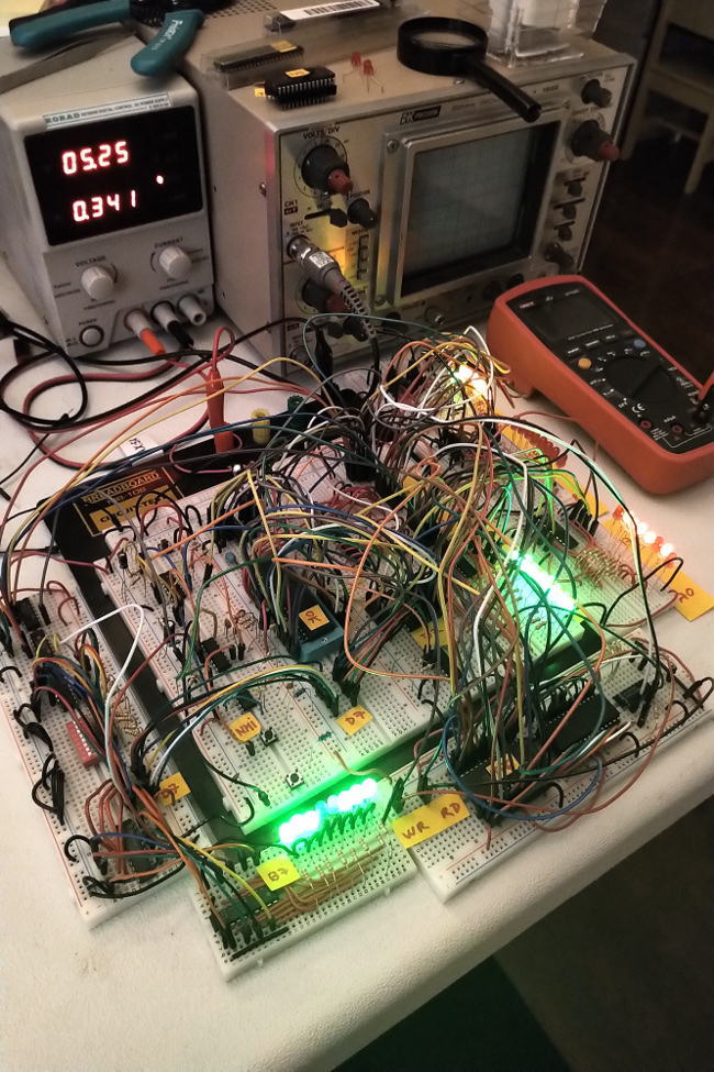
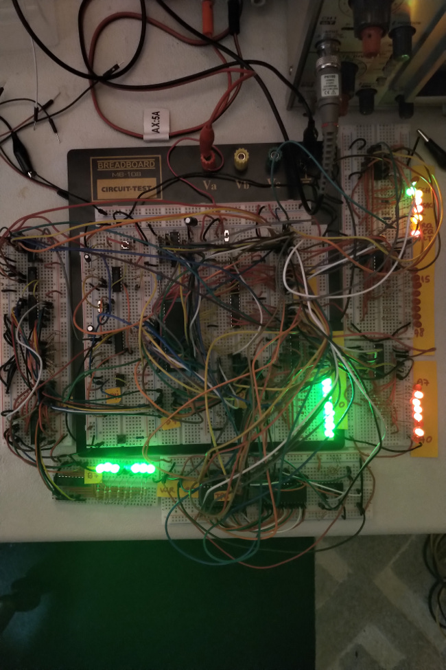
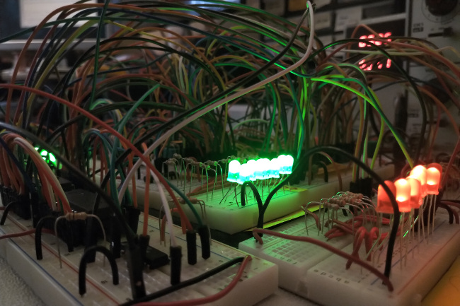
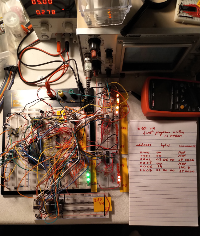
In the image above, you can see the green data bus LEDs. The red LEDs are tied to the address lines A0-A7, through their own 74LS244 buffer (just like the green ones).
The two small breadboards can be considered as external devices, each connected to a CPU bus.
Wired up a 74LS244 to test out logic levels (high and low level voltages) with and without loads.
I had a VERY bad time with a few 22 Ohm resistors that accidentally fell into the 1k Ohm resistor compartment.
Thankfully, the 74LS244 seems ok even after momentarily drawing 40mA more than when unloaded from one output pin with the wrong resistor.
My 74LS244 is actually a Signetics S74LS244N.
From a 5V supply, its unloaded high voltage is 3.7V. Drawing 3mA drops that to 3.4V. Drawing 6mA drops it to 3.35V. Drawing 12mA drops it to 3V, still above the TTL high level output low bound of 2.7V.
Hooked up a 74LS244 to stand in for the buffer for the lower 8 address bits (A0-A7).
day 2
Started planning the breadboard layout to bring in a unidirectional buffer for A0-A7 and a bidirectional one (transceiver) for D0-D7.
Bought a few breadboard segments because I was running out of space.
day 3
Wired up a 74LS245 (actual model is DM74LS245N) to data lines D0-D7.
As soon as I did that, my power supply shot up to the (rather conservative) current limit of 120mA.
I shut it down immediately and started looking for a short-circuit, or maybe a wrong direction in the 74LS245 (it's all hardwired for now).
I measured the supply current of the 74LS245 and was very surprised to see that it drew 47mA!
I even checked a few different types of 74LS245 and found typical supply current draw specified between 40mA and 90mA.
Now that I think about it, it is about double what the octal buffer 74LS244 draws, which has half the amount of Schmitt Triggers (8 instead of 16).
My DM74LS245N outputs a good high-level voltage of 3.7V (when supplied with 5V).
day 4
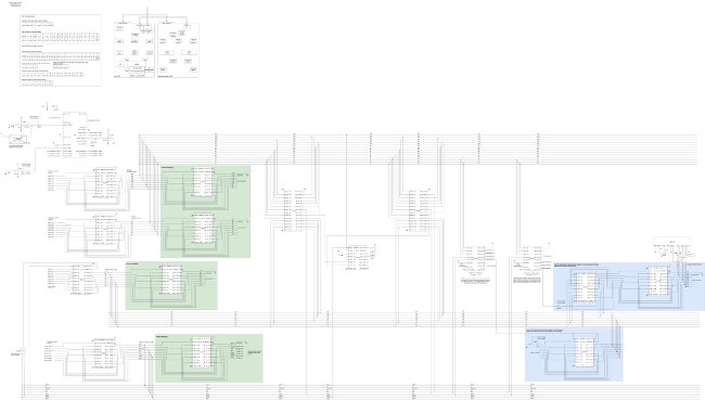
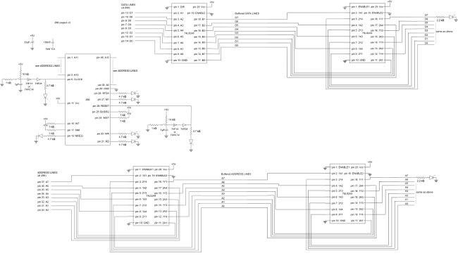
Started drawing up digitally everything I built so far.
day 5
More work on the diagram. I'm also building some small templates to make modifications to the diagram easier.
day 6
More work on the diagram. It has many lines now.
day 7
Wired up indicator LEDs to the data bus as well. They are treated like any other device connected to that bus in that they're behind their own buffer. This minimizes the risk of voltage dropping outside of TTL levels when more devices will be connected to the data bus.
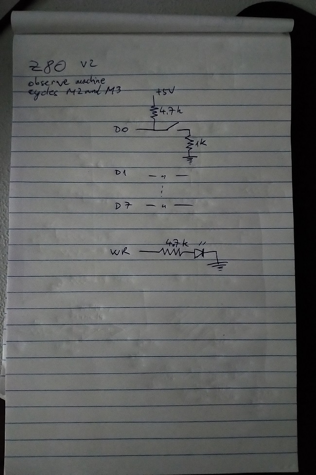
The current-limiting power supply came in handy. With only pull-up resistors near the DIP switches, as soon as the CPU enabled its data lines (for writing), they short-circuited to ground. I shut off the power quickly enough to avoid damage. I followed up immediately with resistors near ground to avoid this.
Hooked up DIP switches to control data lines.
CPU enters a bad state AFTER successfully executing any instruction which reads an operand from memory (e.g.: JP nn).
NOP still works well; I can execute many of them sequentially.
day 2
I've tried with a more complex instruction, JP nn. This should branch unconditionally to the address in nn (2-byte). This would becomes observable on the address lines as soon as JP nn finishes executing.
For some reason, only the first JP nn executes successfully. ANY other instruction that comes after fails (e.g.: NOP, JP nn, etc.)
day 3
Traced and recorded all outputs after the successful first instruction.
It looks like the CPU goes into a bad state and never finishes the M1 (opcode fetch machine cycle) of the second instruction.
If I wired something up incorrectly, I'm surprised JP nn's M2 (memory read) cycles complete successfully.
Changed some resistors, removed some components to try to eliminate the source of failure, without success.
What makes this strange is that the first instruction is always successful, and the second always fails.
day 4
Tried a different Z80 CPU and concluded that the first one was faulty.
The good CPU not only draws significantly less current, but also shows high-level voltages that are closer to 5V on its output pins.
day 5
Tested a few more instructions, including ones that write to the data lines.
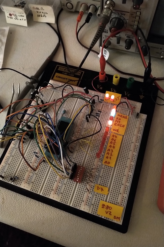
Since I don't yet have a proper bus built, I added resistors at ground (series with switches), along with the pull up resistors, to ensure no short circuits happen when the CPU enables its data pins (low impedance, "write" mode).
When reading from "memory" - that is, my switches - CPU pins are high impedance ("read" mode), so that's not an issue in that case.
A while back I created a game for the ZX Spectrum, during which I learned Z80 assembly language. The purpose here was to delve deeper, learn how it worked, and make this CPU do something interesting - but in the absence of a full-blown commercial computer built around it!
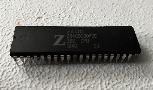
The Zilog Z80 is an 8-bit data, 16-bit address microprocessor released in the late 1970s. It had a variety of applications from personal computer main processor to sound processor in handheld gaming consoles, and was also used in graphing calculators, industrial control.
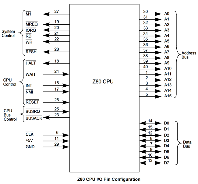
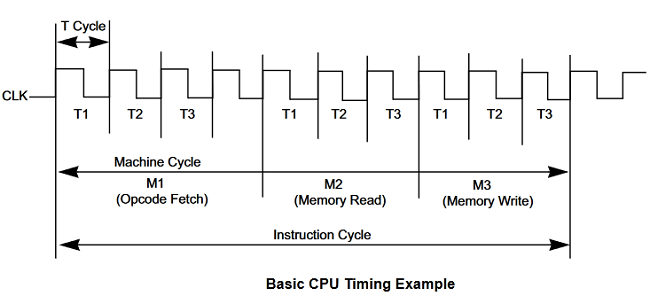
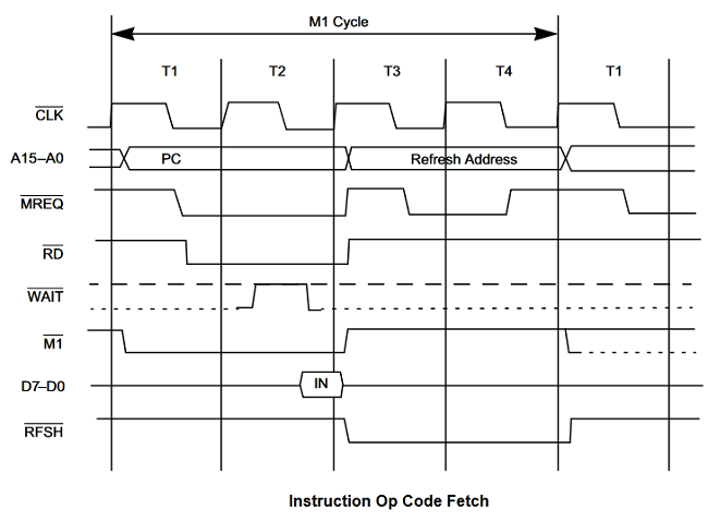
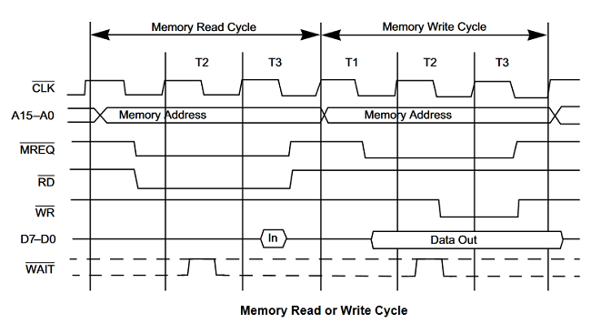
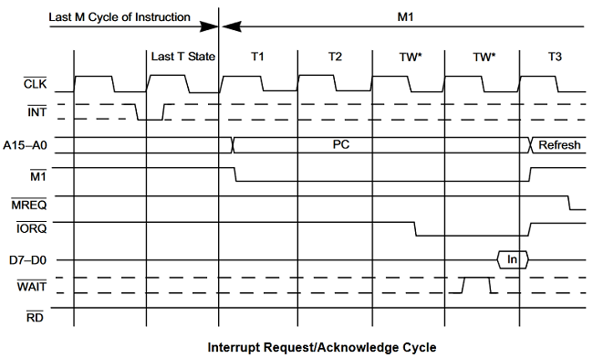
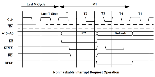
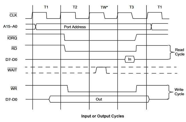
I wanted to perfectly match observed behaviour to Z80 specifications - such as CPU outputs to timing diagrams, clock cycle by clock cycle. This would serve as verification for my setup.
For clock and reset, I've used 74F series ICs because of their compatibility with the older 74 series and their more immediate availability.
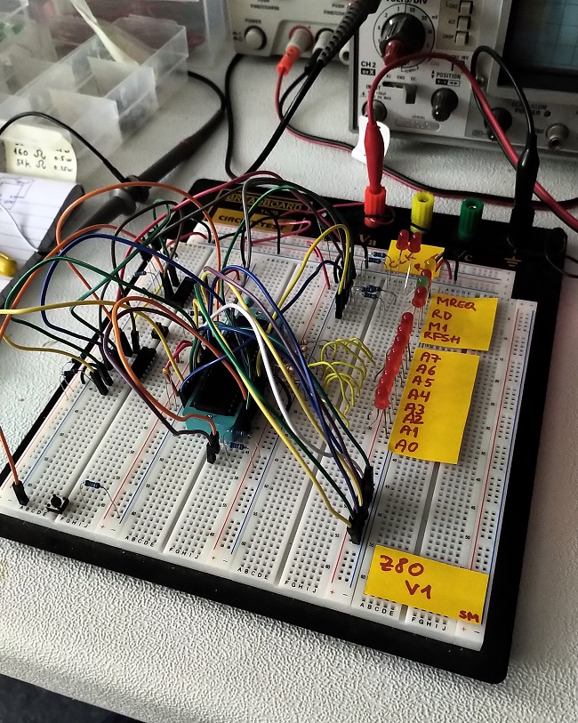
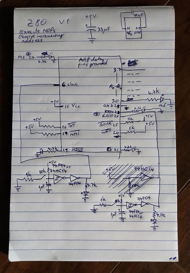
Tried out a CMOS 4584 schmitt trigger IC (plus an inverter) to get some clean edges from a push button.
The 4584 did nothing until I gave it a pull-down resistor.
day 2
Connected all data pins to ground (00000000b = NOP) and first few data pins (D0-D7) to LEDs.
This is equivalent to the program:
0000 NOP
0001 NOP
0002 NOP
etc.
Note: RESET has to stay active (low) for at least 3 clocks, so while I hold down the RESET push button, I have to clock it a few times as well.
Issue: clock signal is dirty - it has to be much cleaner
Issue: address seems to be incrementing, but not cleanly... probably because of the dirty clock
Issue: sometimes the CPU freezes (clocking stops incrementing address)
Note: CPU enters a strange state (garbage on the address lines) if clock line stays low for too long. This may be related to its expectation of the clock line being high during a power down (when HALT is active) state.
day 3
Changed clock to be pulled high and with a capacitor I get much better (90% accurate) debouncing.
I also added an inverter in series with Schmitt and the CPU no longer locks up.
Address increments are not always clean; CPU seems to output junk every now and then.
day 4
Switched Schmitt from a 4584 to a 74HC14 and inverter from a 4069 to a 74F04.
Now the CPU increments the address cleanly, once every 4 clocks.
day 5
I tested without the inverter on the clock pin and it causes CPU to be erratic again, so I'll keep it on.
day 6
After much headache, I learned that timing diagrams graphs show voltage levels and NOT logical levels.
This cleared up confusion around active-low Z80 outputs.
day 7
Reorganized the board to create more space.
Added further LEDs for CPU outputs, clock, etc.s
day 8
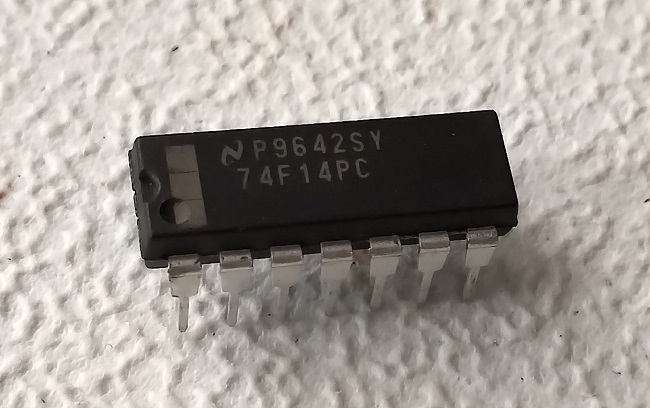
Replaced 74HC14 with 74F14 (to match the inverter 74F04).
I also tried 7414 and that behaved strangely.
For now, I will keep using 74F14 and 74F04.


It started with a simple hardwired setup around the Z80 processor, which kept growing in scope, to a computer with RAM and ROM, and which could interface with external devices, through the ROM code I wrote.
Version 11
In this version I've added a LCD display to seb80. Specifically, it's the LCD 16x2 module, which I've used before, albeit via its 8-bit interface. I wanted to be able to type on my keyboard and have something happen on a display.This time I've opted to change to LCD1602's 4-bit interface, so that I could wire it up to a single I/O port. Aside from the 4 data lines, 2 additionsal lines are used for REGSEL (register select) and ENABLE.
This involved some code changes from the code I wrote back when I interfaced the LCD with Snowdrop OS, on top of the port from x86 to Z80 assembly language.
ROM version 1 binary
ROM version 1 source


Log
day 1Refreshed memory of how to interface a LCD 16x2.
I realized that if I restrict the set of characters I can display on the LCD, I can use only 6 data lines, reserving 2 for control (ENABLE and REGSEL-register select).
Looking at digits 0 through 9 and letters a through z:
ASCII  decimal  binary

0       48     0011 0000

..

9       57     0011 1001


a       97     0110 0001

..

z      122     0111 1010
it is clear that to display all of these, LCD's D7 can be hardwired low and D5 can be hardwired high.
This means that CPU's D7 can be used for ENABLE and D5 for REGSEL.
day 2
Yesterday's plan won't work. During initialization, the LCD controller needs multiple data lines including D7 and D5. This means that I cannot simply hardwire them.
The bad news is that a second latch is needed. The good news is that the entire ASCII character set will be available.
Spent one hour troubleshooting why output to the LCD was garbled and unstable.
The issue was that the latch IC (74LS373) was missing its connection between pin 1 (OUTPUT) and ground.
seb80 can now write to a simple display! This was accomplished by porting my x86 LCD code to Z80.
day 3
I'm going to try using the LCD controller in 4-bit mode. It's somewhat more complex, but it would save me components.
Converted the driver code to use 4-bit mode, eliminating a few ICs and an output device port.
day 4
Soldered everything needed for the display.
Found out the hard way that machined male pin headers make poor contact with regular female pin headers.
This required desoldering of the LCD's machined pin headers, replacing them with regular ones.
Fixed an issue whereby the 10 kOhm resistor I used to bring R/W low was causing the LCD to no longer initialize. The solution was to hardwire R/W directly to ground.
day 5
Updated diagram.
day 6
Started work on ROM updates, around keyboard and display functionality.
day 7
Wrote a scan code to ASCII conversion routine.
day 8
Wrote functionality for reading user input into a buffer.
Version 10
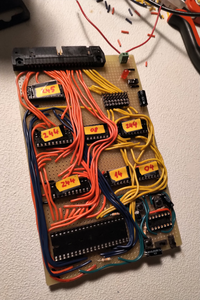
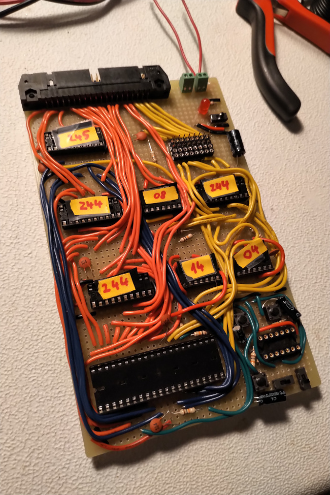
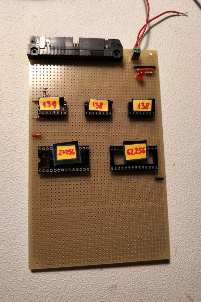
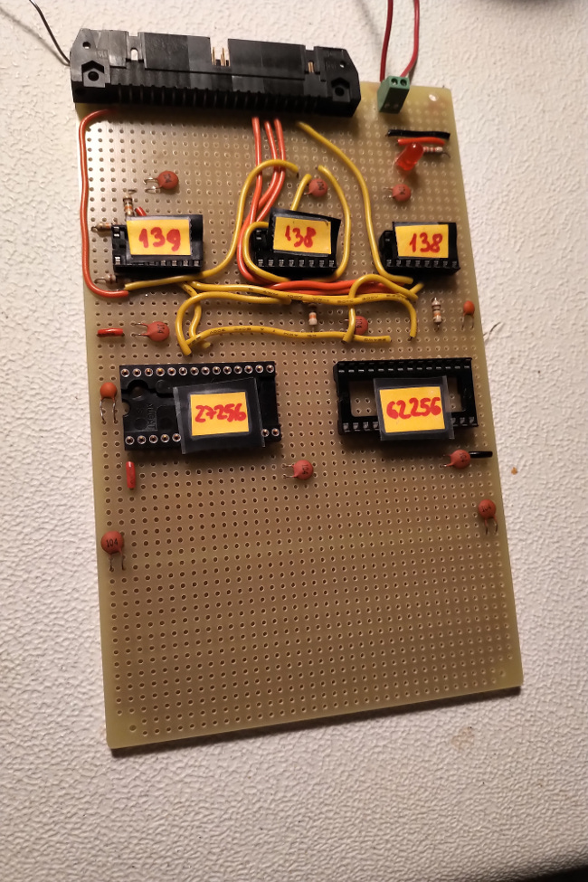
This version took me significantly longer than prior ones. Most of the work here was split between planning PCB layout and actually soldering the computer.All ICs are placed in sockets, to make it easy to replace if they get damaged. I've used higher-quality machined sockets for those which might be replaced more routinely: the ROM and the oscillator.
The computer proper is made up of two boards: CPU board and memory/expansion board. The computer also has built-in 4 input device selectors and 4 output device selectors, to reduce the amount of external circuitry needed for these first 8 devices.
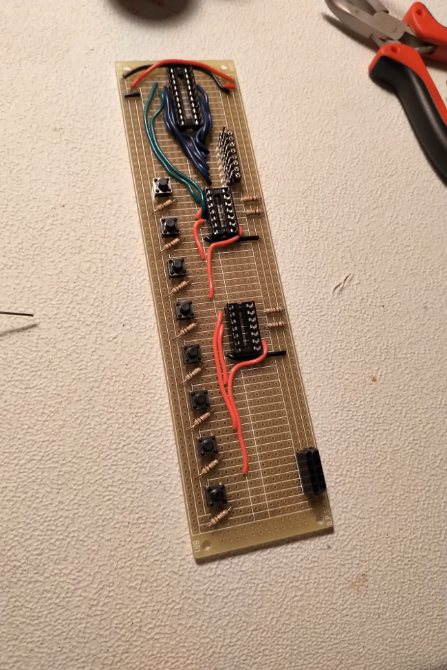
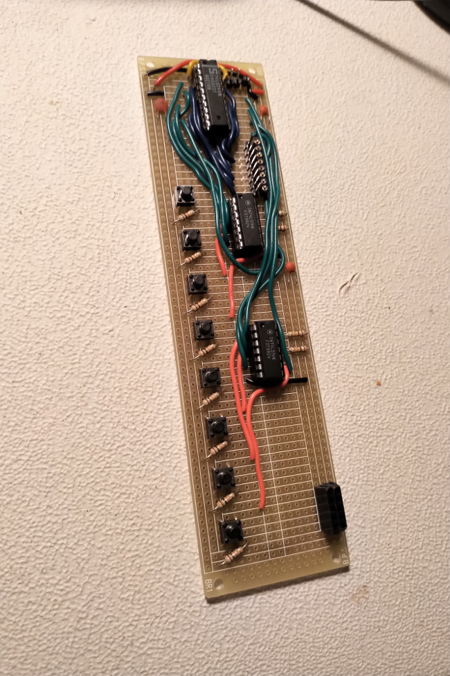
I've built two simple devices on their own PCBs. One is a latch/interface board. It latches data written to it via OUT instructions, making it available to a consumer device via a set of pin headers. Eight on-board LEDs display this latched data, which makes the board useful for debugging, as well.
The second device is a minimalistic keyboard, which uses 8 push buttons. 7 bits are available to compose a "key", while the last button is used as a latch. ROM software reads in the 7 bits only when the latch bit goes high (is pressed).
At this time, its ROM (version 0) simply writes to the output device whenever a value is latched by the user on the keyboard.
ROM version 0 binary
ROM version 0 source


Log
day 1The crystal oscillator needs its own power switch, or it freezes the CPU, even if not connected to the clock pin.
Started designing the CPU PCB.
I'm using electrical tape to fix IC sockets and switches onto the PCB first.
I've started with the CPU and clock.
day 2
Work continues on planning the layout of the CPU PCB.
I've decided to use higher-quality (and more expensive) machined sockets for the ICs that will be more often removed and re-inserted (such as EPROM and oscillator).
day 3
The layout is mostly decided on and soldering has begun.
I'm starting with the CPU board, which is the more difficult one - due to the multitude of connections.
I've started with the clock, reset, and NMI circuits.
day 4
Soldering continues.
The clock, reset, and NMI circuits are all connected to the 40-pin Z80 socket.
Soldered all IC sockets entirely.
Also soldered edge connector entirely. It was difficult due to everything being so close together and having to jump traces.
Burned my fingers twice and stabbed one deeply enough to bleed.
day 5
More soldering, moved on to CPU's control lines.
day 6
More soldering, moved on to CPU's address lines.
day 7
More soldering, the CPU control (output) lines are now connected all the way to the edge connector.
I have decided to bring the pin headers (for external connections) onto the CPU board, since it was not only convenient, but I had some spare room on it.
This also reduces the amount of wires running across the secondary (memory/extension) board by 20-25%.
day 8
More soldering, moved on to CPU's data lines.
day 9
More soldering, moved on to bringing the address lines to the edge connector.
day 10
With the addition of a few bypass capacitors, the CPU board is complete for now.
I'm moving on to the memory/expansion board.
Soldered the edge connector and all IC sockets on the memory/expansion board.
day 11
Another day of soldering, another bloody finger.
Started with all bypass capacitors, since I think it's easier to add them first, to run all wires on top of them, as they lay flat.
Moved on to memory chip and I/O device selectors.
Soldered all inputs to the selectors, as well as all control lines for RAM and ROM.
day 12
Updated diagram with PCB details (connectors, etc.)
Started preparing all pin headers for the expansion points (2 male and 2 female pins for each address line, data line, 4 input devices, 4 output devices).
day 13
Finished preparation of pin headers; I now have all necessary segments.
Soldered address and data expansion pin headers. It was stressful, since there was such a high density of connections.
Soldered ROM to expansion.
The plan is to solder RAM to expansion, and then ROM to edge connector.
day 14
Ceramic disc capacitors have very sharp pins. I found this out while getting another bloody finger.
Soldered RAM to expansion.
Soldered the 4 input device selectors and 4 output device selectors.
Added all connectors to diagram.
day 15
Soldered RAM and ROM to edge connector, which connects all components to the address and data buses.
Added a few power connectors for any external devices to be supplied easily.
Added a PCB layout diagram to the overall diagram.
day 16
These IC sockets are strong. The RAM one gave me 5 inline stabs while trying to pry the IC out of it.
The time I spent carefully checking all connections has paid off: the computer worked "out of the box"!
My first test was with a simple infinite loop at address 0: JP 0
I was able to match the M1/RD timing I observed on the oscilloscope, with one I recorded earlier.
The one from before used a 0.1 MHz clock; its edges were clean, and its high/low levels stable.
This one uses a 3.63 MHz clock; its edges are clearly affected by stray capacitance. Its high/low levels are impacted by - most likely - crosstalk in the ribbon cable, showing as much as a 0.5 V fluctuation in what should be constant high level voltage. Low level fluctuation is smaller, at around 0.3 V.
I'm glad the TTL standard has enough slack built in.
New issue: IORQ, WR seem to not output correctly, staying high past the 74LS244 buffer. This causes the I/O output device selector to not function at all.
This took a few hours to troubleshoot, and it was a combination of issues.
First, IORQ and WR did output correctly. It was just impossible to see on the oscilloscope, as the low state lasted such a short time compared to everything else.
Second, latched output was in fact correct, although initially it seemed fast enough to mean that the latch was in its pass-through state at all times. The issue is that I had reused a program which I wrote (and tested) with a significantly slower clock speed (perhaps 1 kHz), whereas now the clock is at 3.6864 MHz. This and the above made it seem like the latch was always pass-through because IORQ and WR stayed high (inactive).
Third, to make things more difficult, I damaged a Z80 - most likely by discharging static electricity into it. The air in the room is quite dry this time of year. I have to be more careful around these CPUs.
Fourth, it seems like channel 2 of my oscilloscope is sometimes malfunctioning. For some reason it won't pick up voltage changes, except at high frequencies.
After a few modifications to the program, I can clearly see IORQ and WR on the oscilloscope as well.
day 17
Brought over the NTSC signal generation circuit and tested it successfully.
Next, I will create a latch device which can be used as a generic output device, based on the 74LS373. Its outputs will be buffered via a 74LS244.
Wasted an IC socket after choosing a cheap PCB whose traces had unintended contacts.
Decided to use a good PCB rather than a cheap one.
day 18
Finished soldering the latch device on a PCB.
This device offers 8-bit data output that is latched when a byte is written to its hardware I/O port.
Any consumer device can rely on this to receive data from the Z80 reliably.
Bonus: because I had room on the board, I also connected 8 LEDs to the outputs. This makes it excellent for debugging - for example, the value of the accumulator can be written to it and then observed by a human.
From the specs, the 74LS244 can source 15 mA from a logical high output pin (more from a logical low). I've measured the green LEDs at 2.3 V and they're in series with 2.2 kOhm. From the 74LS244's measured logical high of 3.2 V, the LEDs consume about 0.4 mA, leaving quite a bit for a low-power device to draw directly from this latch board.
day 19
Started work on the computer's first input device.
It's based on 8 push buttons, each hardware-debounced via a Schmitt trigger.
I expect to use one of the switches as the "latch", so that it's easy to interface this device by polling.
day 20
More soldering on the keyboard.
day 21
Finished soldering the keyboard.
Updated diagram.
day 22
The computer is now officially named seb80 (intentionally all lowercase). It sounds a bit like "zed eighty", the CPU.
Laid the foundation for seb80's ROM.
It will feature a collection of useful routines, including delays, keyboard, etc.
Wrote a keyboard routine which will register latches and return both whether something was just latched and current hardware button state.
This proves that the keyboard module works - and it works the first time!
I am very pleased that for the amount (I approximate around 1000 points) of soldering I have done, everything worked the first time; no soldering fix-ups were needed. Much of that is owed to the time I spent updating and verifying the diagram, as well as on-going continuity testing after each batch of connections I soldered.
day 23
Finished up ROM development for this version.
Version 9
I have restricted the scope of this version to generating luminance-only NTSC signal. This results in grayscale-only output, black to white. Chrominance signal is significantly more difficult to implement, and requires higher clock frequencies than those at which my breadboard prototype computer can operate.Anything faster than the 3.6864 MHz crystal oscillator I ultimately chose caused system instability.
Generating stable NTSC frames requires consistent timing. Visible scan lines need to have their horizontal sync pulses at the same time, to prevent image distortion (shearing, rolling, etc.) The number of invisible, vertical sync scan lines varies significantly from TV to TV.
The interfacing circuit is very simple. Given that NTSC televisions have a terminating 75 Ohm resistor at their input, it was simple to design a Y resistor network connected to two pins of an output device. Pin 0 had 1k Ohm and pin 1 had 470 Ohm. Approximately, 00b output 0V (sync), 01b output 0.3V (black), 10b output 0.7V (gray), 11b output 1V (white).


I've used program NTSC2 to get consistent scan line timing, before setting out to display anything on a television set yet.
Programs NTSC4 and NTSC5 below are complete examples of generating static images, as well as dynamic images, based on modifications made by a user via an input.
NTSC4 program - generates a static image
NTSC5 program - generates a vertical bar which can be moved with a button


NTSC4 program listing
;
; program NTSC4
;
; purpose: generate a static NTSC frame
;
; IMPORTANT: all of these timings are specific to a
;            CPU clock frequency of 3.6864 MHz
;
JP start

; data region
colours:
DB 2, 3, 2, 1, 3, 1, 2, 3, 2

start:
LD C, 06h            ; output port
LD A, 1
LD E, 242

OUT (C), A           ; start with front porch level of 0.3V
NOP
NOP
NOP                  ; a small initial front porch

;
; visible scan line loop: generate 242 visible vertical scan lines
;
new_scanline:
; here, output is 0.3V
; here, register E contains remaining visible scan line count
; here, register C contains output port number
; here, register A contains 1
; (since logical 1 outputs 0.3V: front porch level)
                     ; here we're on the front porch

DEC A                ; 4 clocks
                     ; A := 0 (preparing to output 0V for horizontal sync)
OUT (C), A           ; 12 clocks
                     ; falling edge to 0V (logical 0)

                     ; we're now at the start of horizontal sync

INC A                ; 4 clocks, still at 0V
                     ; A := 1, preparing to output 0.3V
OUT (C), A           ; 12 clocks, rising edge to 0.3V (logical 1)
                     ; signal has now risen to the level of the
                     ; back porch

                     ; TOTAL TIME ON HORIZONTAL SYNC
                     ;                   4 + 12 = 16 clocks

                     ; we're at the start of the back porch
                     ; and have risen to 0.3V (logical 1)


; front porch took: 30 clocks
; back porch took: 19 clocks
; horizontal sync took: 16 clocks
; total invisible: 65 clocks
;
; 1 clock = 1 / 3.6864 MHz = 0.271267361us
; total scan line: 63.55us / 0.271267361us = 234.27 clocks per line
;                                            round down to 234
; remaining for visible region: 234 - 65 = 169 clocks
; NOTE: visible region starts on back porch

; IMPORTANT:
;     output voltage is now 0.3V from the back porch
;     available visible region MUST NOT change that output for
;     another 19 clocks

                     ; we're still on back porch

; BEGIN 169 clock area

LD A, R              ; 9 clocks, NOOP instruction

LD HL, colours       ; 16 clocks
                     ; HL := pointer to colour array

OUTI                 ; 16 clocks
                     ; output byte at address in HL to port C
                     ; B := B - 1
                     ; HL := HL + 1
                     ; this changes colour being output and
                     ; advances colour pointer

                     ; NOTE: the back porch can be longer, if
                     ;       available visible area begins
                     ;       with black
                     ;       this 19 clock internval represents
                     ;       the minimum time needed for back porch

                     ; we're now on the available visible region

OUTI                 ; 16 clocks
OUTI                 ; 16 clocks
OUTI                 ; 16 clocks
OUTI                 ; 16 clocks
OUTI                 ; 16 clocks
OUTI                 ; 16 clocks
OUTI                 ; 16 clocks
OUTI                 ; 16 clocks

; END 169 clock area

; end of available visible region

; here, register C contains output port number
                     ; we're still in visible region
                     ; assume register C contains output port number

LD A, 1              ; 7 clocks, still in visible region
OUT (C), A           ; 12 clocks, signal 0.3V (logical 1)

                     ; 7 + 12 = 19 clocks taken out of visible region
                     ; to set up front porch voltage

                     ; we're now at the start of the front porch

                     ; 14 clocks (from jumping to start of loop)
                     ; plus
                     ; 4 + 12 = 16 clocks (from setting up
                     ; horizontal sync at beginning of loop)

                     ; TOTAL TIME ON FRONT PORCH
                     ;                14 + 16 = 30 clocks

DEC E                ; 4 clocks
JP NZ, new_scanline  ; 10 clocks
                     ; E-- and next visible scan line
                     ; this spends an additional 14 clocks on front porch


; we've now completed all visible scan lines
; the timing of the last line is short by:
;     16 clocks spent setting up 0V for the start of the horizontal sync

; here, register C contains output port number
; here, register A contains 1
; (since logical 1 outputs 0.3V: front porch level)

LD E, 2              ; 7 clocks
                     ; setup vertical blanking line counter
                     ; NOTE: there might be great variability
                     ;       in televisions here; mine worked
                     ;       better with a low value, rather
                     ;       than the value of 20 from specification

DEC A                ; 4 clocks
                     ; A := 0 (preparing to output 0V vblank)
OUT (C), A           ; 12 clocks
                     ; falling edge to 0V (logical 0)

; first vblank line will run 7 clocks longer (1.9us)

                     ; we're now at the start of vblank
                     ; (right after horizontal sync)
;
; vertical blanking loop: generate several invisible vertical
;                         sync lines (inverted horizontal sync)
;
new_vblank_line:
; here, register E contains remaining vertical blanking line count
; here, register C contains output port number

                     ; we're now at the start of the vblank portion
                     ; outputting 0V

; 19 clocks to set up horizontal sync
; 16 clocks spent on horizontal sync
; 27 clocks pre-empting values in case we are jumping to visible
;           lines loop
; 16 clocks spent counter decrement/jump to start of loop
; 19 + 16 + 11 + 16 = 62 total clocks for housekeeping
;
; 234 clocks per line
; 234 - 62 = 172 clocks left for computation
;

; BEGIN 172 clock area

LD IX, (0000h)       ; 20 clocks (NOOP instruction)
LD IX, (0000h)       ; 20 clocks (NOOP instruction)
LD IX, (0000h)       ; 20 clocks (NOOP instruction)
LD IX, (0000h)       ; 20 clocks (NOOP instruction)
LD IX, (0000h)       ; 20 clocks (NOOP instruction)

LD IX, (0000h)       ; 20 clocks (NOOP instruction)
LD IX, (0000h)       ; 20 clocks (NOOP instruction)
LD IX, (0000h)       ; 20 clocks (NOOP instruction)

NOP                  ; 4 clocks
NOP                  ; 4 clocks
NOP                  ; 4 clocks

; END 172 clock area

LD A, 1              ; 7 clocks, still in vblank portion
OUT (C), A           ; 12 clocks, signal 0.3V (logical 1)
                     ; 7 + 12 = 19 clocks spent in vblank

                     ; we're now at the start of horizontal sync

                     ; it's inverted for vertical blanking
                     ; interval (0.3V instead of 0V)

DEC A                ; 4 clocks
                     ; A := 0
OUT (C), A           ; 12 clocks, signal 0V (logical 0)
                     ; 4 + 12 = 16 clocks spent on horizontal sync

                     ; we're now at the start of vblank portion

LD B, 242            ; 7 clocks
INC A                ; 4 clocks
                     ; A := 1, B := 242, HL := ptr to colour data
                     ; pre-empt the values needed by visible
                     ; scan line loop, in case we're
                     ; done with the vertical blanking
                     ; 7 + 4 = 11 clocks
                     ; NOTE: this IS wasteful, but is done this
                     ;       way to keep timing consistent
                     ;       and not have to unroll loops

DEC E                ; 4 clocks
                     ; vertical blanking line counter--
JR NZ, new_vblank_line
                     ; 12 clocks when jumping
                     ; 7 clocks when not

; now return to visible scan line loop to begin a new video frame

; here, register B contains remaining visible scan line count
; here, register C contains output port number
; here, register A contains 1

; here, we're 5 clocks short on the last vertical blanking line
OUT (C), A           ; 12 clocks, signal 0.3V (logical 1)
                     ; we're now on the front porch of first
                     ; visible scan line

LD E, B              ; 4 clocks
                     ; prepare visible line loop

JP new_scanline      ; 10 clocks
; last vertical blanking line runs 11 clocks long (2.98us)
; first visible scan line sees a front porch 1 clock longer (0.27us)
Log
day 1Bought a 3.6864 MHz oscillator crystal metal package. Period is 0.271267361us.
I first had to figure out the pinout, since the only data sheet I found for this RASCO PLUS oscillator was unclear which pin was which.
I was happy to see that the computer runs well at a frequency into the megahertz, since so far the fastest I've run it was around 1 kHz.
This is because I have so many long wires everywhere on the breadboard, that I thought stray capacitance would add enough noise for the CPU to be unstable.
One thing I'm noticing is that the CPU freezes if I try to clock it manually while the oscillator is active (though not inputting into the CPU's clock pin).
I found a way to work around this: power off the oscillator and the manual clock will work fine.
day 2
My plan is to re-visit a project from university.
While most of courses in university were computer science (theory, programming, etc.), one of the most enjoyable was ECE385H: Microprocessor Systems. It was a lab-heavy course in which we interfaced various components together.
One of the lab projects involved using an Atmel microcontroller to generate timing accurate enough to create a steady image on a television screen. The circuitry needed was minimal: a purpose-built resistor network acting as a DAC to input into a television set's analog coaxial input.
The driver program was written in C and the timing of our program (when to write various values to an output port) had to respect the NTSC standard closely enough to generate a black-and-white image.
This is what I wish to re-create here - this time not using a microcontroller and C, but using my own custom Z80 computer.
This time, I think that I'll have the extra advantage of more precise timings for my loops, etc., due to writing the driver program in Z80 assembly language - thus having the benefit of knowing exactly how many clocks (T-states) each instruction will take.
day 3
Began timing planning.
Each NTSC video frame draws 242 visible scan lines and 20 invisible scan lines ("vertical blanking").
visible scan line timing


region              NTSC duration     voltage


horizontal sync     4.7us             0V

back porch          4.5us             0.3V

front porch         1.5us             0.3V


entire invisible    10.7us

entire scan line    63.55us

entire visible      52.85us           0.3V to 1V
invisible scan line timing ("vertical blanking")


region              NTSC duration     voltage


horizontal sync     4.7us             0.3V

vblanking period    58.85us           0V
NOTE: Since front and back porches are at black-level voltage (0.3V), I can extend their durations, to be a bit safer.
The cost of this is reduced horizontal resolution (since some of the left and right edges will always be black), which I accept.
My main concern (looking at these timings) is to generate a short and accurate horizontal sync pulse - since that's the shortest transition of all durations.
If the 0V level is represented by logical 0, then I can have the 0.3V level be represented by logical 1.
The following is my first timing prototype for repeatedly generating scan lines.
This is meant to be observed on an oscilloscope, since it has no vertical blanking interval - just hardcoded scan lines.
day 4
First attempt at scan line timing was promising: entire scan line is about 0.55us short, front porch and back porch are about 5us too long.
I have also tried running this breadboard computer from a 10 MHz crystal oscillator and it was unstable, so I abandoned it for now.
It will probably work well once I build the computer on PCBs, but there's just too much interference on the breadboards (long wires, etc.)
Found a suitable command-line assembler. The programs are becoming too large to type in hex values by hand.
day 5
Spent some more time adjusting the visible scan line loop.
Converted the program from an infinite loop to a finite one, performing 242 iterations - one for each visible scan line.
Added the vertical blanking interval line loop. This is where calculations and changing memory will take place, so that the visible scan line loop is as fast as possible.
Added a CMOS inverter to get output voltages closer to supply and 0.
Hooked up to a television (resistor values 1000Ohm on pin 0 and 470Ohm on pin 1) and I'm seeing an image for the first time!
Problems: top of the screen is sheared and gray-coloured bar looks black.
Removed the CMOS inverter and used the TTL outputs of the 74LS244 buffer directly. This made the gray bar visible!
At this point, something is not synchronizing properly, and I believe it's the vertical.
I don't think it's the horizontal because the lines that are NOT sheared are output by the exact same loop and look fine.
Reduced the vertical blanking line count from 20 to 10. Sheared region is smaller.
Reduced the vertical blanking line count from 10 to 5. Sheared region is smaller.
day 6
Reduced the vertical blanking line count from 5 to 2. Sheared region is smaller.
For displaying vertical bars, I found that using OUTI and re-initializing HL to point to the start of a colour array is the fastest.
The image is static and stable. The program which generates it is called NTSC4.
day 7
Started work on a program that updates something on the screen when an input device changes state.
day 8
Finished NTSC5, the program which moves a vertical line on screen whenever a button is pressed.
Version 8
To create a way to input from a device, I used a second 74LS138 3-to-8 decoder as well as a 74LS244, which becomes enabled only when the specific device is read. When this happens, the 74LS244 gains control of the data bus, writing to it.The input device I built is a segment of 8 DIP switches.
TP6 - test program for I/O input
Log
day 1This begins part 2 of interfacing with I/O devices; in this version I want to add the necessary circuitry to be able to input from devices.
Just like for output devices, a 74LS138 3-to-8 decoder (part is SN74LS138N) will be used to enable one of up to four input devices.
Already, I/O devices at port 4, 5, 6, 7 (A2=1) are be output devices.
Thus, I/O devices at port 0, 1, 2, 3 (A2=0) will be input devices.
NOTE: for input devices that won't rely on these built-in selectors, care has to be taken that they are wired to ports whose A2=1, to not conflict with the built-in input device selectors which expect A2=0.
Input devices:


A2  A1  A0

C   B   A  Y

0   0   0  Y0  input device at port 0

0   0   1  Y1  input device at port 1

0   1   0  Y2  input device at port 2

0   1   1  Y3  input device at port 3
day 2
The second 74LS138 was easy to design; it's just like the output one, except being enabled by Z80's RD line (along with IORQ).
The switches will be buffered by a 74LS244, enabled by one of the input device selector's outputs.
day 3
Wired up the input selector 74LS138.
Wrote TP6, a test program to test input via a device made up of switches:
Address  Bytes            Mnemonic

0000                      ; TP6

0000                      ; test program for I/O input

0000                      ;

0000                      ; the reason for these is to verify that

0000                      ; the input device selector remains inactive

0000                      ; during outputs

0000   3E 81              LD A, 10000001b

0002   D3 04              OUT (04h), A

0004   3E C3              LD A, 11000011b

0006   D3 05              OUT (05h), A

0008   3E E7              LD A, 11100111b

000A   D3 06              OUT (06h),A

000C   3E FF              LD A, 11111111b

000E   D3 07              OUT (07h),A

0010   3E 00              LD A, 0

0012   D3 06              OUT (06h), A  ; clear LEDs

0014                      ; now read from the four input devices, to

0014                      ; verify correct signals from the input

0014                      ; device selector

0014   DB 00              IN A, (00h)   ; reads garbage when not connected

0016   DB 01              IN A, (01h)   ; reads garbage when not connected

0018   DB 02              IN A, (02h)   ; reads garbage when not connected

001A            READ_SWITCHES:

001A   DB 03              IN A, (03h)   ; read switches

001C   D3 06              OUT (06h), A  ; display value on LEDs

001E   C3 1A 00           JP READ_SWITCHES
Verified that the 74LS138 correctly selects an input device, as wired.
Wired up the 74LS244. It was much easier than before, with the extensive wiring diagram I've been maintaining.
Program TP6 ran successfully, demonstrating the full I/O cycle (read from DIP switches, write to LEDs).
Version 7
I made my first steps into I/O device interfacing. The test I/O output device I created consists of LEDs which display the last value written to the device's port.The device's entry point is a 74LS373 octal d-type latch which snapshots the data bus when enabled. It is enabled by one of the outputs of a 74LS138 3-to-8 decoder, which serves as an output device selector.
The latch output is buffered by a 74LS244, which provides sufficient current for the LEDs.
See the log below for program listings.
TP4 - test program for I/O output
TP5 - increment-and-output test program for I/O

Log
day 1Began designing the I/O circuit. My plan is to expose selectors for eight different I/O devices via a 74LS138 3-to-8 decoder (part is SN74LS138N).
Wiring this up to A0-A2 will allow easy access to I/O ports 0 through 7.
For the prototyping stage (on the breadboard), I want to wire up and output device made up of 8 LEDs which will display the last value written to the respective I/O port.
I realized that by adding a second 74LS138 3-to-8 decoder I could expose 4 input and 4 output devices with no further chips.
One 74LS138 will rely on Z80's RD line to become enabled and the other will rely on Z80's WR line to become enabled.
Address line A2 will select between the first 4 and the next 4.
I/O devices at port 0, 1, 2, 3 (A2=0) will be input devices.
I/O devices at port 4, 5, 6, 7 (A2=1) will be output devices.
NOTE: for input devices that won't rely on these built-in selectors, care has to be taken that they are wired to ports whose A2=1, to not conflict with the built-in input device selectors which expect A2=0.
Output devices:
A2  A1  A0

C   B   A  Y

1   0   0  Y4  output device at port 4

1   0   1  Y5  output device at port 5

1   1   0  Y6  output device at port 6

1   1   1  Y7  output device at port 7
day 2
Wired the 74LS138 which will select between four output devices.
Wrote TP4, my first I/O output test program.
Address  Bytes                Mnemonic


0000                          ; TP4

0000                          ; test program for I/O output

0000                          ;

0000     3E 81                LD A, 10000001b

0002     D3 04                OUT (04h), A

0004     3E C3                LD A, 11000011b

0006     D3 05                OUT (05h), A

0008     3E E7                LD A, 11100111b

000A     D3 06                OUT (06h), A

000C     3E FF                LD A, 11111111b

000E     D3 07                OUT (07h), A

0010     C3 00 00             JP 0000h
Verified with a multimeter that the output device selector (74LS138) works as intended.
Since the main breadboard is running out of room, I've brought out the data lines onto a side breadboard.
Designed the first output device: 8 LEDs.
It's based on 74LS373 (part is DM74LS373N) octal d-type latch (transparent). While this latch has the advantage of having a level-sensitive LE (latch enable), it is active high, unlike all other TTL chips I've used so far. Luckily, my 74LS04 hex inverter still has some free slots.
The I/O output device selector was already tested, so all I had to do is connect a small breadboard which already had LEDs and a 74LS244 buffer wired up.
Wrote program TP5, below, which is supposed to successively write higher values to an output device, with visible delay. NMI should reset the value to 0.
Address  Bytes                  Mnemonic


0000                            ; TP5

0000                            ; second test program for I/O output

0000                            ;   increment value written to output port (with

0000                            ;   visible delay)

0000                            ;   NMI clears counter to zero

0000                            ;

0000     3E 00                  LD A, 0

0002     32 0F F0               LD (0F00Fh), A        ; counter := 0

0005                  MAIN_LOOP:

0005                            ; here, A = counter value

0005     D3 06                  OUT (06h), A          ; output counter value

0007     01 DE 08               LD BC, 2270           ; busy wait iteration count

000A                  DELAY:

000A     0B                     DEC BC                ; 4 clocks

000B     78                     LD A, B               ; 4 clocks

000C     B1                     OR C                  ; 4 clocks

000D                                                  ; (MSB OR LSB) = 0?

000D     C2 0A 00               JP NZ, DELAY          ; 10 clocks

0010                                                  ; no, keep looping

0010     21 0F F0               LD HL, 0F00Fh

0013     34                     INC (HL)

0014     3A 0F F0               LD A, (0F00Fh)

0017     C3 05 00               JP MAIN_LOOP

001A     FF FF ...              DB 76 DUP (0FFh)      ; pad up to NMI handler start

0066                  NMI_HANDLER:

0066     3E 00                  LD A, 0

0068     32 0F F0               LD (0F00Fh), A        ; counter := 0

006B     ED 45                  RETN                  ; return from NMI
The program ran successfully! The counter was observable on the LEDs of the output device and NMI successfully reset the counter to zero.
day 4
Updated diagram
Version 6
Version 6 introduces an oscillator clock and a manual NMI circuit (activated via push button) alongside the manual, push button NMI. To test both NMI and INT interrupts, I wrote three programs.See the log below for program listings.
TP1 - test program for NMI
TP2 - test program for INT
TP3 - second test program for NMI


Log
day 1Wired up a 555 circuit.
I did it much faster than the last time I worked with a 555, probably because of the few hundred connections I've made for the Z80.
day 2
Replaced the last two 74F series chips with 74LS, to rely exclusively on the 74LS family of TTL logic ICs.
Broke a pin on one CPU and discovered that another one was faulty (internal short-circuit).
That means I'm down to two good CPUs.
Re-wired the manual clock ICs and introduced a switch which selects between manual clock and 555-driven clock.
This has allowed me for the first time to observe instruction timing on an oscilloscope.
day 3
Reset is now automatic. I used a simple RC circuit to make the RESET pin start low at power-on and reach 2V after a generous 0.8 seconds - giving enough low-level time for three clocks, ensuring a successful reset.
It will also feature a push button to allow manual reset as well, for the cases when clock is manual or just to reset more easily partway through program execution.
day 4
Designed a "generate NMI" button. I debounced it just like the clock button, to prevent multiple NMIs from being generated on a push.
Wrote TP1, the NMI test program.
address  bytes                mnemonic

0000                          ; TP1

0000                          ; test program for NMI

0000                          ;   loops while NMI routine has not run

0000                          ;   enters infinite loop after NMI routine runs

0000                          ;

0000   31 00 90               LD   SP,9000h    ; stack bottom (NMI needs stack)

0003   3E 00                  LD   A,0

0005   32 FF FF               LD   (0FFFFh),A  ; hasNmiRun := FALSE

0008                WAIT_NMI:                  ; do

0008   3A FF FF               LD   A,(0FFFFh)

000B   FE 00                  CP   0

000D   CA 08 00               JP   Z,WAIT_NMI  ; while !hasNmiRun

0010                AFTER_NMI:

0010   00                     NOP

0011   C3 10 00               JP   AFTER_NMI   ; infinite loop

0014   FF FF ..               DB 82 DUP (0FFh) ; pad up to NMI routine start

0066                NMI_ROUTINE:

0066   3E 01                  LD   A,1

0068   32 FF FF               LD   (0FFFFh),A  ; hasNmiRun := TRUE

006B   ED 45                  RETN             ; return from NMI
Program was verified successfully! Before NMI is generated, the CPU loops between 0008 and 000D. After NMI is generated, the CPU enters the infinite loop at 0010.
day 5
Changed all pull-up resistors in my design to 10k for consistency's sake.
I'm going to test INT interrupt signals with a bouncy push button. For fun, I will be able to see how many bounces each push generated.
Wrote TP2, the INT test program.
address  bytes                mnemonic

0000                          ; TP2

0000                          ; test program for INT

0000                          ;   infinite loop which reads a variable which holds

0000                          ;       a count of generated INT signals

0000                          ;   INT routine increments count variable

0000                          ;

0000   31 00 90               LD   SP,9000h    ; stack bottom (INT needs stack)

0003   21 0F F0               LD   HL,0F00Fh

0006   36 00                  LD   (HL),0      ; initialize counter

0008   ED 56                  IM   1           ; choose interrupt mode 1,

000A                                           ; which assumes that the

000A                                           ; interrupt handler is at 0038

000A   FB                     EI               ; enable interrupts

000B                READ_COUNT:

000B   21 0F F0               LD   HL,0F00Fh

000E   7E                     LD   A,(HL)      ; read INT count

000F   C3 0B 00               JP   READ_COUNT  ; infinite loop

0012   FF FF ...              DB 38 DUP (0FFh) ; pad up to INT handler start

0038                INT_HANDLER:

0038   21 0F F0               LD   HL,0F00Fh

003B   34                     INC   (HL)       ; count++

003C   ED 4D                  RETI             ; return from INT
Verified that the counter is incremented when an interrupt signal is raised.
Made a second test program for NMI, to count invocations.
address  bytes                mnemonic

0000                          ; TP3

0000                          ; a second test program for NMI

0000                          ;   infinite loop which reads a variable which holds

0000                          ;       a count of generated NMI signals

0000                          ;   NMI handler increments count variable

0000                          ;

0000   31 00 90               LD   SP,9000h    ; stack bottom (NMI needs stack)

0003   21 0F F0               LD   HL,0F00Fh

0006   36 00                  LD   (HL),0      ; initialize counter

0008                READ_COUNT:

0008   21 0F F0               LD   HL,0F00Fh

000B   7E                     LD   A,(HL)      ; read INT count

000C   C3 08 00               JP   READ_COUNT  ; infinite loop

000F   FF FF ...              DB 89 DUP (0FFh) ; pad up to NMI handler start

0066                NMI_HANDLER:

0066   21 0F F0               LD   HL,0F00Fh

0069   34                     INC   (HL)       ; count++

006A   ED 45                  RETN             ; return from NMI
Successfully observed NMI incrementing the counter variable.
Version 5
Version 5 introduces RAM via the Hitachi HM62256LP-70 32kb RAM IC. Since both RAM and ROM are implemented via 32kb chips, no address decoding is necessary. Line A15 is used to switch between the two (low means ROM, high means RAM).This maps memory addresses 0000-7FFF to ROM and 8000-FFFF to RAM.
To test my new setup, I've written a program which reads and writes (to RAM only) to the edges of RAM and ROM. I've asserted that the setup was valid by observing the data line LEDs as the Z80 read values from memory - and then comparing to my expectation.
See the log below for the program listing. You can also download the 32kb ROM binary here.


Log
day 1Validated my expectation that for IO writes, the Z80 keeps correct write data on its data lines past IORQ/WR returning to their inactive state.
This means that interfacing with D-type flip-flops should be reasonably easy.
My plan is to use them for a built-in, write-only device made up of 8 LEDs which I'll use for debugging, by simply OUTputting byte values (which get latched) to it.
day 2
Started planning and diagramming the integration of the RAM chip. I'm using a Hitachi HM62256LP-70.
This is nice: the HM62256's pinout is very similar to the 27C256's.
By placing the RAM chip next to the ROM chip on the breadboard, I was able to bring address and data to the RAM chip neatly, using some very short jumper wires.
The RAM chip is fully wired up except for its control lines, which I still have to design.
I've hardwired its control (CS, OE, WE) high (inactive), so that I can still test that the ROM works well.
day 3
Designed final connections of data bus transceiver (74LS245) and settled on a chip select strategy.
Wired the 74LS245 transceiver to be enabled and disabled by the Z80, depending on MREQ and IORQ (when either becomes active). This was done simply with a 74LS08 AND gate.
Wired the 74LS245 transceiver to have its direction controlled by the Z80 via direct connection to Z80's RD line.
This many breadboards are dropping some voltage, so I've increase supply to 5.1V.
day 4
Designed the memory chip selection circuit. It will simply split on A15 between a 32k RAM chip and a 32k ROM chip.
This way all memory registers are uniquely addressable and all memory registers are addressable
For both RAM and ROM, OE (output enable) lines are connected directly to the RD line on the bus.
For RAM, WE (write enable) line is connected directly to the WR line on the bus.
To select one of RAM and ROM, I've used a 74LS139 1-of-4 decoder (also called 2-to-4). The exact part is DM74LS139.
The 74LS139 is enabled by Z80's MREQ. Its A input is tied to Z80's A15. Its B input is hardwired high.
day 5
Wired everything, moving previous connections to the ROM onto the decoder.
Ran the program below successfully, verifying reading from end of ROM, as well as writing and then reading from beginning and end of RAM:
Address   Bytes                Mnemonic


0000                           ; TP0

0000                           ; test program for RAM/ROM interfacing

0000                           ;

0000      3A FF 7F             LD a, (7FFFh)       ; verify last byte of ROM

                                                   ; (see end of listing)

0003      3E E5                LD a, 11100101b

0005      32 00 80             LD (8000h), a       ; write magic value to

                                                   ; first byte of RAM

0008      32 FF FF             LD (0FFFFh), a      ; write magic value to

                                                   ; last byte of RAM

000B      AF                   XOR a

000C      3A 00 80             LD a, (8000h)       ; verify first byte of RAM

000F      AF                   XOR a

0010      3A FF FF             LD a, (0FFFFh)      ; verify last byte of RAM

0013      C3 00 00             JP 0000h

0016      FF FF FF FF FF ...   DB 32745 DUP (0FFh) ; fill up ROM

7FFF      0F                   DB 0Fh              ; last byte of ROM
Assertions were done via the LD a, (MMMM) statements, where I verified that the data lines contained the proper byte that was expected to exist in memory at the specified address. I also measured the output of the decoder to verify that it was activating the expected memory chip each time.
day 6
Brought diagram up to date.
Version 4
Version 4 is important because it introduces memory. To that end I used the 27C256-25 EPROM. Its capacity is 256kbit, or 32kbyte. This means that it's addressable via 15bit addresses. This further means that I will be able to use A15 (the sixteenth address line) as a chip selector between the 27C256 ROM and whatever RAM chip I choose. A 74LS32 OR gate was used to connect Z80's RD and MREQ to 27C256's CE and OE pins.The EPROM required significant investment into an EPROM programmer (or burner - I got MCUmall's GQ-4x4 v4) and an EPROM UV eraser (also from MCUmall). I also ran out of space on my existing breadboards and had to buy several segments.
Running the first program from memory was very satisfying.


Log
day 1Wired up the high 8 bits of the address bus and the 8 bits of the data bus.
All can now be observed via the 16+8 LEDs.
I decided to stick to my current plan of a 74LS244 dedicated to each set of LEDs. This is because even with moderate current, high level voltage output by the 74LS244 that drives the LEDs can drop by 0.2V. I want this to be isolated away from the buses.
Basically, I'd rather add components than have surprises later with the memory, etc., because of inadequate high level voltages.
day 2
Wired up all unused inputs into the ICs used for manual reset and clock.
day 3
Wired up the buffered control lines (CPU outputs).
At this point all control, address, and data lines can be observed via LEDs.
day 4
I am getting ready to connect a ROM to the existing circuit.
First, I had to clean up some breadboard room. It's getting quite busy and I was running out of room on my desk.
I'm going to be using a 27C256-25 EPROM. This is a 256kbit (32kbyte) UV-erasable EPROM.
A few weeks ago I purchased a MCUmall GQ-4x4 EPROM programmer as well as a UV eraser tool, in anticipation for this stage.
day 5
Added the ROM and its connections to the diagram.
Allocated a new breadboard piece for the ROM.
Since there's no RAM (thus no writing to memory) yet, I chose the simplest way to wire up the ROM, combining Z80's MREQ and RD lines through a 72LS32 OR gate, outputting to 27C256's CS and OE lines.
Installed drivers for the EPROM burner inside a Windows XP 32bit virtual machine.
First burn was of a 32k buffer containing only 0x14, which translates to INC D.
Hooked it up and the data bus LEDs are showing an incorrect value.
Instead of 00010100b, it's showing 00101000b, which translates to a conditional relative jump.
This explains why the PC seems to be jumping around randomly, instead of a steady increment as a result of executing the one-byte INC D.
Tried with 0xC3 (11000011b) which worked fine - probably because it's palindromic.
Something is wired backwards.
day 6
Although the data bus LEDs show D7 at the top (consistently with A15, A7 at the top of their LED groups), the data bus itself is wired backwards, with D7 at the bottom.
Rewired the ROM chip and labelled the two inconsistent D7s. This wasn't easy - the breadboard is spaghetti.
I came up with a nice way to protect the pins of the ROM chip. I keep it always inserted into a 28-pin DIP socket, even when I erase it in the EPROM eraser. On the breadboard, the DIP socket is plugged into a pair of pin header strips to stabilize it on the breadboard. This way, the ROM pins are static.
First program:
Address   Bytes        Mnemonic


0000:     00           NOP

0001:     00           NOP

0002:     C3 06 00     JP 0x0006

0005:     00           NOP

0006:     14           INC D

0007:     C3 00 00     JP 0x0000
First attempt at running it failed. It incorrectly read a 0xFF at address 0002.
I checked in the EPROM burner and it's read successfully.
Fixed wire-ups: A0-A3 were wired incorrectly as A3-A0 at LEDs
Fixed wire-ups: A0-A3 were wired incorrectly as A3-A0 at address bus
These two "wrongs" made the "right" of the LEDs displaying expected addresses, despite them being wrong on the bus (and consequently at the ROM).
day 7
I'm testing and still having at least two data lines wired incorrectly somewhere.
Fixed wire-ups: swapped O2 and O5 at ROM.
First program executed successfully from ROM, for the first time!
Version 3
My time on version 3 was split into three equal parts: first, research a unidirectional buffer for the address bus and a bidirectional buffer for the data bus. To this end, I've used 74LS244 and 74LS245, respectively. Second, start building these connections on the breadboard, along with some LEDs for the data bus. Third, create a diagram on the computer to replace the one in my notebook.
In the image above, you can see the green data bus LEDs. The red LEDs are tied to the address lines A0-A7, through their own 74LS244 buffer (just like the green ones).
The two small breadboards can be considered as external devices, each connected to a CPU bus.
Log
day 1Wired up a 74LS244 to test out logic levels (high and low level voltages) with and without loads.
I had a VERY bad time with a few 22 Ohm resistors that accidentally fell into the 1k Ohm resistor compartment.
Thankfully, the 74LS244 seems ok even after momentarily drawing 40mA more than when unloaded from one output pin with the wrong resistor.
My 74LS244 is actually a Signetics S74LS244N.
From a 5V supply, its unloaded high voltage is 3.7V. Drawing 3mA drops that to 3.4V. Drawing 6mA drops it to 3.35V. Drawing 12mA drops it to 3V, still above the TTL high level output low bound of 2.7V.
Hooked up a 74LS244 to stand in for the buffer for the lower 8 address bits (A0-A7).
day 2
Started planning the breadboard layout to bring in a unidirectional buffer for A0-A7 and a bidirectional one (transceiver) for D0-D7.
Bought a few breadboard segments because I was running out of space.
day 3
Wired up a 74LS245 (actual model is DM74LS245N) to data lines D0-D7.
As soon as I did that, my power supply shot up to the (rather conservative) current limit of 120mA.
I shut it down immediately and started looking for a short-circuit, or maybe a wrong direction in the 74LS245 (it's all hardwired for now).
I measured the supply current of the 74LS245 and was very surprised to see that it drew 47mA!
I even checked a few different types of 74LS245 and found typical supply current draw specified between 40mA and 90mA.
Now that I think about it, it is about double what the octal buffer 74LS244 draws, which has half the amount of Schmitt Triggers (8 instead of 16).
My DM74LS245N outputs a good high-level voltage of 3.7V (when supplied with 5V).
day 4
Started drawing up digitally everything I built so far.
day 5
More work on the diagram. I'm also building some small templates to make modifications to the diagram easier.
day 6
More work on the diagram. It has many lines now.
day 7
Wired up indicator LEDs to the data bus as well. They are treated like any other device connected to that bus in that they're behind their own buffer. This minimizes the risk of voltage dropping outside of TTL levels when more devices will be connected to the data bus.
Version 2
One difficulty I encountered here was that I had a faulty chip. This caused many hours of frustration and debugging, thinking that my setup was causing the issue. See log for more information.The current-limiting power supply came in handy. With only pull-up resistors near the DIP switches, as soon as the CPU enabled its data lines (for writing), they short-circuited to ground. I shut off the power quickly enough to avoid damage. I followed up immediately with resistors near ground to avoid this.
Log
day 1Hooked up DIP switches to control data lines.
CPU enters a bad state AFTER successfully executing any instruction which reads an operand from memory (e.g.: JP nn).
NOP still works well; I can execute many of them sequentially.
day 2
I've tried with a more complex instruction, JP nn. This should branch unconditionally to the address in nn (2-byte). This would becomes observable on the address lines as soon as JP nn finishes executing.
For some reason, only the first JP nn executes successfully. ANY other instruction that comes after fails (e.g.: NOP, JP nn, etc.)
day 3
Traced and recorded all outputs after the successful first instruction.
It looks like the CPU goes into a bad state and never finishes the M1 (opcode fetch machine cycle) of the second instruction.
If I wired something up incorrectly, I'm surprised JP nn's M2 (memory read) cycles complete successfully.
Changed some resistors, removed some components to try to eliminate the source of failure, without success.
What makes this strange is that the first instruction is always successful, and the second always fails.
day 4
Tried a different Z80 CPU and concluded that the first one was faulty.
The good CPU not only draws significantly less current, but also shows high-level voltages that are closer to 5V on its output pins.
day 5
Tested a few more instructions, including ones that write to the data lines.
Since I don't yet have a proper bus built, I added resistors at ground (series with switches), along with the pull up resistors, to ensure no short circuits happen when the CPU enables its data pins (low impedance, "write" mode).
When reading from "memory" - that is, my switches - CPU pins are high impedance ("read" mode), so that's not an issue in that case.


Version 1
Although most of the years I've spent coding in assembly language focused on the x86 CPU, the Z80 is near and dear to my heart. The reason for this is the computer (ZX Spectrum) that got me started in the world of software relied on a Z80 CPU.A while back I created a game for the ZX Spectrum, during which I learned Z80 assembly language. The purpose here was to delve deeper, learn how it worked, and make this CPU do something interesting - but in the absence of a full-blown commercial computer built around it!
The Zilog Z80 is an 8-bit data, 16-bit address microprocessor released in the late 1970s. It had a variety of applications from personal computer main processor to sound processor in handheld gaming consoles, and was also used in graphing calculators, industrial control.

This is version 1 of my project, and I've kept it simple. My goal was to get a manually-clocked Z80 to execute the simplest instruction, NOP, while observing an incrementing PC (program counter) to ever higher addresses.
I wanted to perfectly match observed behaviour to Z80 specifications - such as CPU outputs to timing diagrams, clock cycle by clock cycle. This would serve as verification for my setup.
For clock and reset, I've used 74F series ICs because of their compatibility with the older 74 series and their more immediate availability.

Clock
A push button is used to generate clock signals. Its signal is cleaned up by a Schmitt trigger, to ensure clean edges. By default the clock is held high, since I discovered that when held low for a long time, the CPU can enter an undefined state.Reset
Another push button is used to bring the RESET line low (active) to reset the CPU. It too has its edges cleaned by a Schmitt trigger.Address lines
The first 8 of 16 address lines (A0-A7) are connected to LEDs, to allow easy observation of the incrementing PC (program counter) value. I've used 4.7k Ohm resistors (to LEDs), since A0-A7 are not really meant to drive anything.Data lines
All 8 data lines (D0-D7) are wired low. The CPU sees this as a NOP (value 0) instruction. This is great for testing because it allows the CPU to only require machine cycle 1 (M1), which is 4 clock cycles long. This is because no memory accesses are needed by NOP.Outputs
I've only sampled a few outputs (also via 4.7k Ohm resistors to LEDs) - enough to trace the CPU through the spec timing diagram of the 4-clock cycle M1.


Log
day 1Tried out a CMOS 4584 schmitt trigger IC (plus an inverter) to get some clean edges from a push button.
The 4584 did nothing until I gave it a pull-down resistor.
day 2
Connected all data pins to ground (00000000b = NOP) and first few data pins (D0-D7) to LEDs.
This is equivalent to the program:
0000 NOP
0001 NOP
0002 NOP
etc.
Note: RESET has to stay active (low) for at least 3 clocks, so while I hold down the RESET push button, I have to clock it a few times as well.
Issue: clock signal is dirty - it has to be much cleaner
Issue: address seems to be incrementing, but not cleanly... probably because of the dirty clock
Issue: sometimes the CPU freezes (clocking stops incrementing address)
Note: CPU enters a strange state (garbage on the address lines) if clock line stays low for too long. This may be related to its expectation of the clock line being high during a power down (when HALT is active) state.
day 3
Changed clock to be pulled high and with a capacitor I get much better (90% accurate) debouncing.
I also added an inverter in series with Schmitt and the CPU no longer locks up.
Address increments are not always clean; CPU seems to output junk every now and then.
day 4
Switched Schmitt from a 4584 to a 74HC14 and inverter from a 4069 to a 74F04.
Now the CPU increments the address cleanly, once every 4 clocks.
day 5
I tested without the inverter on the clock pin and it causes CPU to be erratic again, so I'll keep it on.
day 6
After much headache, I learned that timing diagrams graphs show voltage levels and NOT logical levels.
This cleared up confusion around active-low Z80 outputs.
day 7
Reorganized the board to create more space.
Added further LEDs for CPU outputs, clock, etc.s
day 8
Replaced 74HC14 with 74F14 (to match the inverter 74F04).
I also tried 7414 and that behaved strangely.
For now, I will keep using 74F14 and 74F04.
Z80 diagrams
Here are some useful diagrams, including the Z80 pinout, timing diagrams, etc.


27C256 EPROM diagrams
Here are some useful diagrams, including pinout, timing, etc.

62256 RAM diagrams
Here are some useful diagrams, including pinout, timing, etc.